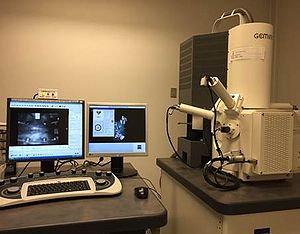
Specific Process Knowledge/Characterization/SEM Supra 1
THIS PAGE IS UNDER CONSTRUCTION
Feedback to this page: click here

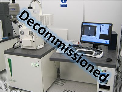
SEM LEO

The SEM LEO is a scanning electron microscope. It is a very reliable and rugged instrument that provides high quality SEM images of most samples, and it has excellently served the users of the cleanroom for many years. Excellent images on a large variety of materials such as semiconductors, semiconductor oxides or nitrides, metals, thin films and some polymers may be acquired on the SEM.
However, the SEM LEO has now been equipped with a Raith e-beam lithography system, and from the turn of the year 2015-2016 it is exclusively dedicated to the users of the Raith E-beam lithography, so system so general imaging of user samples is no longer allowed.
The SEM LEO was installed in the cleanroom in the 1998, and the software was ungraded in 2012.
The user manual, control instruction, the user APV and contact information can be found in LabManager:
SEM LEO info page in LabManager,
Performance information
| Equipment | SEM LEO (Leo 1550 SEM) | |
|---|---|---|
| Purpose | Imaging and measurement of |
|
| Other purpose |
| |
| Location |
| |
| Performance | Resolution |
The resolution is strongly dependent on the type of sample and the skills of the operator. |
| Instrument specifics | Detectors |
|
| Stage |
| |
| Electron source |
| |
| Operating pressures |
| |
| Options |
| |
| Substrates | Batch size |
|
| Allowed materials |
| |
