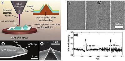
LabAdviser/Technology Research/Organic Ice Resists for Electron-Beam Lithography - Instrumentation and Processes
Ice Lithography for Advanced Nanofabrication
- Project type: Ph.D. project
- Project responsible: William Tiddi
- Sites involved: DTU Danchip,
Project description

Physical dimension of integrated circuits keep shrinking at exponential rates, due market demand for faster, more powerful, longer-lasting and more compact electronic devices. Standard fabrication techniques manage to keep up the pace, but need to resort to extremely expensive equipment, increased fabrication complexity and intense research for dedicated chemicals satisfying the tightening process constraints. Ice lithography is a nanopatterning technique derived from electron beam lithography, showing feature resolution below 10nm. A thin ice layer condensed on the sample takes the role of the lithographic resist film when exposed to electron or ion beams. This process is immensely cheaper and more sustainable than state-of-the-art techniques relying on physical masks and aggressive chemistries. Our goal is to investigate ice lithography and the steps it needs to be ported from research to future industry, establishing its potential as the break-through technology needed to advance further in the ultra large scale integration semiconductor roadmap.
Want to know more?
- https://www.youtube.com/watch?v=_8OvbTUIUNs
- King, G.M. et al., 2005. Nanometer patterning with ice. Nano Letters, 5(6), 1157–1160.
- Han, A. et al., 2011. An ice lithography instrument. Review of Scientific Instruments, 82(6), 065110.
- Han, A. et al., 2012. Nanopatterning on nonplanar and fragile substrates with ice resists. Nano Letters, 12(2), 1018–1021.
