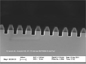
Specific Process Knowledge/Etch/III-V ICP/GaAsnano
Appearance
Feedback to this page: click here
GaAs nano etch
| Recipe | GaAs Nano Etch |
| Cl2 flow | 4 sccm |
| Ar flow | 12 sccm |
| Platen power | 80 W |
| Coil power | 700 W |
| Pressure | 6 mTorr |
| Platen chiller temperature | 20 oC |
| Results (GaAs Nano Etch) | |
| GaAs | 5 nm/s |
| AlInP | 1 nm/s |
| HSQ | 1.5 nm/s |
| ZEP520a | 2 nm/s |
| Si3N4 | 2 nm/s |
 |
|---|
