Specific Process Knowledge/Lithography/EBeamLithography
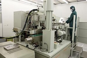
The JEOL JBX-9500 electron beam lithography system is a spot electron beam type lithography system designed for writing patterns with dimensions from nanometers to sub-micrometers. The minimum electron beam is around 12 nm, the maximum writitng field without stitching is 1 mm x 1 mm.

The machine is located in a class 10 cleanroom (E-2) with tight temperature and moisture control. The room must only be entered when the machines or equipment inside the room is intended to be used.
Performance of the e-beam writer
| Purpose | pattern an electron sensitive resist | Mainly for pattering structures with minimum feature size between 20 nm - 1 µm |
|---|---|---|
| Performance | Resolution |
|
| Maximum writing area without stitching |
| |
| Process parameter range | E-beam voltage |
|
| Scanning speed |
| |
| Min. electron beam size |
| |
| Min. step size |
| |
| Beam current range |
| |
| Dose range |
| |
| Samples | Batch size |
Wafer cassettes:
|
| Substrate material allowed |
|
Getting started
To request a training session or a time-slot for the e-beam, contact the e-beam team via this link: e-beam@danchip.dtu.dk'
You need 3-4 training sessions before being allowed to use the e-beam writer. You can get training in loading and unloading samples into a cassette, to optically pre-align the samples, to calibrate the writer, to perform 2nd alignment and start exposure. For safety reasons, the costumer is however not allowed to load or unload cassettes to or from the e-beam writer.
Before you request for a training, it is crucial to have your pattern ready in either tdb-format or GDSII format. Also, check your pattern in e.g. CleWin before requesting. In order to reach the files from the computers inside the cleanroom, it is recommended to either dropbox them or send them per email to yourself.
It is also recommended to gather as much knowledge about your e-beam run from your colleagues, i.e. which e-beam current, aperture and dose to use, which shot pitch (e.g. SHOT A,10). In order to get an overview of what an e-beam process requires, it is recommended to a assist a fully trained colleague of yours when she or he e-beam writes. Furthermore, please read the e-beam manual for more information on which parameters to use.
On the L-drive, a logbook for the e-beam writer can be found. Sheet 1 gives you an overview of which condition files (currents and apertures) have been in use recently by which user on which type of resist. On sheet 2 in this logbook you can find a writing time estimation program; please use this prior to requesting e-beam sessions. If in doubt how to use it, contact the e-beam team at [1].
There are 3 manuals for the e-beam writer:
- A user manual describing the standard procedure when e-beam writing
- A jdf-, and sdf-file manual describing how to prepare sdf-, and jdf-files (found under 'Technical Documents')
- A BEAMER manual describing how to convert your pattern file (GDSII-format) to v30-format (found under 'Technical Documents')
Process Flows
ZEP520A is used as a standard positive e-beam resist. A process flow for spinning, e-beam exposing and development of this resist can be downloaded here (word format): Process_Flow_ZEP.docx; please note that the individual steps of the process flow should be optimised to your specific processing technique, this process flow thus being a guideline.
You can use the SSE-spinner, the Manual Spinner 1 or the III-V spinner to coat wafer or chips with e-beam resist. Read more about these spinners
here (opens in a new tab).
- ZEP520A (standard resist), FLOW
- table of available resists
| Resist | ZEP520A | ZEP7000 | PMMA | MMA (AR-P 617.05) | CSAR | HSQ/XR-1541 | Ma-N 2403 | Mr EBL 6000 | AR-N 7520 |
| Polarity | Positive | Positive | Positive | Positive | Positive | Negative | Negative | Negative | Negative
|
| Manufacturer | ZEON | ZEON | AllResist | AllResist | DOW Corning | Micro Resist | Micro Resist | AllResist | |
| Comments | Standard positive resist. Technical Report to be found here: ZEP520A.pdf | Low dose to clear. Used for trilayer (PEC-free) resist-stack. Please contact Lithography. Technical Report to be found here: ZEP7000.pdf | Technical Report to be found here: | Approved, not tested yet. Used for trilayer (PEC-free) resist-stack or double-layer lift-off resist stack. Technical Report to be found here: | Approved, not tested yet. Technical Report to be found here: | Approved, not tested yet. Should work quite similar as ZEP520A. Please contact Lithography. Technical Report to be found here: | Standard negative resist | CC | Negative resist to be tested soon.
|
| Spinner | SSE, Manual Spinner 1, III-V Spinner | Manual Spinner 1, III-V spinner | Manual Spinner 1, III-V spinner | Manual Spinner 1, III-V spinner | Manual Spinner 1, III-V spinner | Manual Spinner 1, III-V spinner | Manual Spinner 1, III-V spinner | Manual Spinner 1, III-V spinner | Manual Spinner 1, III-V spinner |
| Developer | AA | AA | AA | AA | AA | BB | BB | BB | BB |
| Rinse | AA | AA | AA | AA | AA | BB | BB | BB | BB |
| Remover | AA | AA | AA | AA | AA | BB | BB | BB | BB |
| Process Flow (docx-format) | Process_Flow_ZEP.docx | Trilayer stack: Process_Flow_Trilayer_Ebeam_Resist.docx | AA | Trilayer stack: Process_Flow_Trilayer_Ebeam_Resist.docx | AA | BB | BB | BB | BB |
Proximity Error Correction
- PEC in BEAMER
- trilayer flow, not tested
Charge dissipating agent
- Al coating, FLOW
- ESPACER, no flow yet
