Specific Process Knowledge/Characterization/SEM: Scanning Electron Microscopy
Scanning electron microscopy at Danchip
The four SEM's at Danchip cover a wide range of needs both in the cleanroom and outside: From the fast in-process verification of different process parameters such as etch rates, step coverages or lift-off quality to the ultra high resolution images on any type of sample intended for publication.
The 'workhorse' SEM that will cover most users needs is the Leo SEM. It is a very reliable and rugged instrument that provides high quality images of most samples. Excellent images on a large variety of materials such as semiconductors, semiconductor oxides or nitrides, metals, thin films and some polymers may be acquired on the Leo SEM. As such, we prefer that new users that have no prior SEM experience get trained on the Leo SEM before they start using the FEI or Zeiss.
The Zeiss SEM is the newest SEM in the cleanroom. It's a state-of-the-art SEM that will produce excellent images on almost any sample. Operated by the same user interface as the Leo, it is quite straight forward to change between the two instruments.
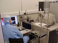
The FEI SEM was acquired to cope with the growing need for polymer related imaging. It is a versatile microscope with two vacuum modes (High Vacuum and Low Vacuum) and 6 different detectors, offering excellent resolution on any type of sample or material. This great performance, however, requires a skilled operator that knows how to achieve it. Also, we have learned that the high degree of sophistication and the great number of detectors make it much less robust compared to the other SEM's. It is therefore the intention that only users with special needs (for instance thick polymers, glass substrates or EDX/micromanipulator experiments) that will be trained. Furthermore, the instrument is equipped with a Oxford Inca EDX system and a Kleindiek micromanipulator with a Capres 4 point probe.
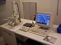
Jeol SEM Outside the cleanroom in the basement of building 347, the Jeol SEM provides a possibilty
- The SEM's at Danchip
-
The FEI SEM
The user manuals, quality control procedures and results, user APVs, technical information and contact information can be found in LabManager:
Process information
- Etch of silicon using RIE
- Etch of silicon oxide using RIE
- Etch of silicon nitride using RIE
- Etch of photo resist using RIE
| Equipment | RIE1 | RIE2 | |
|---|---|---|---|
| Purpose | Dry etch of |
|
|
| Performance | Etch rates |
|
|
| Anisotropy |
|
| |
| Process parameter range | Max pressure |
|
|
| Max R.F. power |
|
| |
| Gas flows |
|
| |
| Substrates | Batch size |
|
|
| Allowed materials |
|
| |
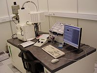
We have four SEM's at Danchip. Together they cover a wide range of needs both in the cleanroom and outside: From the fast in-process verification of different process parameters such as etch rates, step coverages or lift-off quality to the ultra high resolution images on any type of sample intended for publication.
The 'old workhorse' SEM that will cover most users needs is the Leo SEM. It is a very reliable and rugged instrument that provides high quality images of most samples. Due to its robustness new users only need a mandatory two hour training session before they are free to use it by themselves. It is a standard high vacuum instrument equipped with a field emission gun, 3 high vacuum electron detectors (Se2, Inlens and RBSD) and a Röntec EDX system. You can obtain excellent images on a large variety of materials such as semiconductors, semiconductor oxides or nitrides, metals, thin films and some polymers. We prefer that new users that have no prior SEM experience get trained on the Leo SEM before they start using the FEI or Zeiss.

The FEI SEM has been acquired to cope with the growing need for polymer and e-beam related imaging. It is an extremely versatile microscope with two vacuum modes (High Vacuum and Low Vacuum) and 7 different detectors, offering excellent resolution on any type of sample or material. This great performance, however, requires a skilled operator that knows how to achieve it. Also, we have learned that the high degree of sophistication and the great number of detectors make it much less robust compared to the other SEM's. It is therefore the intention that only users with special needs (for instance thick polymers, glass substrates or EDX/micromanipulator experiments) that will be trained. Furthermore, the instrument is equipped with a Oxford Inca EDX system and a Kleindiek micromanipulator with a Capres 4 point probe.
The Zeiss SEM is the newest SEM in the cleanroom.

Jeol SEM The less advanced Jeol SEM offers a great alternative for many types of SEM needs. If you have to check the result of an etch process, a lift-off etc. before you proceed with the process sequence, the Jeol SEM is a much better choice. It is simple, faster to use, has a very low sample exchange time and is by far more accessible than any of the other SEMs. There is a very good chance that it is free when you need it. On heavily charging polymers such as SU-8 it even does a better job than the Leo SEM. To use it, a 1-2 hour training session is necessary.
| SEM - Zeiss | SEM - FEI | SEM - Leo | SEM - Jeol | |
|---|---|---|---|---|
| Model | Zeiss Supra 55 VP | FEI Nova 600 NanoSEM | Leo 1550 SEM | Jeol JSM 5500 LV SEM |
| Electron emitter type | FEG (Field Emission Gun) | FEG (Field Emission Gun) | FEG (Field Emission Gun) | Tungsten filament |
| Vacuum modes | High vacuum (>2*10mbar) and Low vacuum (0.1-1.9 mbar) | High vacuum (>2*10mbar) | High vacuum and Low vacuum | |
| Detectors | High and Low vacuum detectors of SE and BSE electrons, HiVac Inlens SE detector and high resolution Low vacuum detector | SE, Inlens SE and BSE detectors | High vacuum SE and BSE detector | |
| Substrate size | Up to 6" wafer with full view | Up to 6" wafer with 4" full view | Up to 4" wafer with full view | |
| Additional equipment | Kleindiek micromanipulator with Capres 4 point probe | |||
| Best obtainable lateral resolution (strongly dependent on user skills and sample type) | Down to 1-2 nm (Limiting factor: Beam) | Down to 10 nm (Limiting factor: Vibrations) | Down to 20-30 nm (Limiting factor: Vibrations) | |
| General availability | Good | Poor | Excellent | |
| Ease of use | A sophisticated user interface with many features and many different detectors: Complicated | A simple user interface with joystick and a limited number of detectors: Relatively simple | A simple user interface with joystick with one detector: Very simple | |
| User level access | Only experienced SEM users, masters/Ph.D students with special needs will be trained | Any cleanroom user | Any cleanroom user | |
| Best usage | High resolution imaging of any sample | High resolution imaging of any non-polymer sample | Fast in-process imaging | |
| EDX analysis | Oxford Inca system | Röntec system | Not available |

