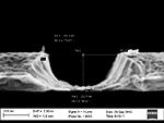
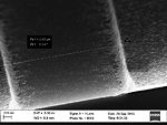
Specific Process Knowledge/Etch/IBE⁄IBSD Ionfab 300/IBE Au etch
Appearance
Feedback to this page: click here
Template:CC-bghe
Results from the acceptance test in February 2011
Acceptance test for Au etch:
| . | Acceptance Criteria |
Acceptance Results |
|---|---|---|
| Substrate information |
|
. |
| Material to be etched |
|
. |
| Mask information |
|
. |
| Features to be etched |
|
. |
| Etch depth |
|
|
| Etch rate |
|
|
| Etch rate uniformity |
|
|
| Reproducibility |
|
|
| Selectivity (Au etch rate/ZEP etch rate) |
|
|
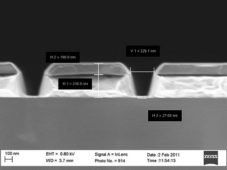
| Etch profile |
|
|
Process parameters for the acceptance test
| Parameter | Au etch acceptance |
|---|---|
| Neutralizer current [mA] | 550 |
| RF Power [W] | 1300 |
| Beam current [mA] | 500 |
| Beam voltage [V] | 600 |
| Beam accelerator voltage | 400 |
| Ar flow to neutralizer [sccm] | 5.0 |
| Ar flow to beam [sccm] | 10.0 |
| Rotation speed [rpm] | 20 |
| Stage angle [degrees] | 30 |
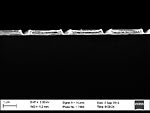
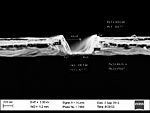
Some SEM profile images of the etched Au
 |
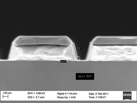 |
IBE Au etch with Ti mask
by bghe@nanolab
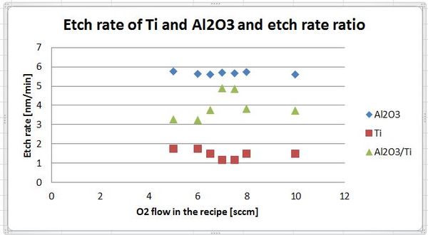
Work has been started to find a good process for etching gold with a Titanium mask with high selectivity.
| Ti etch test with Zep520A as mask - To etch the Ti mask | Au etch test with high selectivity to Ti | |
|---|---|---|
| General description | This recipe has a good selectivity between ZEP520A resist and Ti, which makes it good for patterning the Ti that should be used as masking layer for the Au etch. It can also be used to etch Au if the selectivity to the mask is good enough. | This recipe has especially good selectivity between Ti and Au which makes it good for gold etching using a thin Ti mask as masking layer. The selectivity to resist is very bad so do not use it with a resist mask. |
| Recipe name |
Ti acceptance 20111129 |
Au_acceptance_with_O2 |
| IBE parameters |
|
|
| Results | ||
| Etch rate in resist |
12.8 nm/min (15-12-2011) |
72 nm/min (13-12-2011) |
| Etch rate in Au |
32.7nm/min (15-12-2011) |
42.6nm/min (13-12-2011) |
| Etch rate in Ti |
8.3nm/min (15-12-2011) |
4.3nm/min (13-12-2011) |
| Selectivity Ti/Zep |
0.65 (15-12-2011) |
0.06 (13-12-2011) |
| Selectivity Au/Ti |
3.9 (15-12-2011) |
9.9 (13-12-2011) |
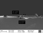
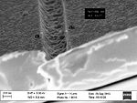
| SEM images of the etch profile (click to view a larger image) |
|
|

