Specific Process Knowledge/Lithography/DUVStepperLithography/DUVStepper
DUV Stepper

Feedback to this section: click here
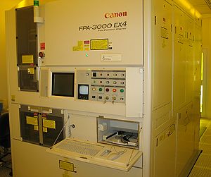
The deep-UV stepper FPA-3000EX4 from Canon is an advanced exposure system designed for mass-production of 6 and 8 inch wafers/ devices having a throughput of up to 90 wafers per hour. The largest applicable thickness of the wafers/ devices is 1,2 mm. Also 4" wafers/ devices can be processed with some restrictions concerning throughput, resolution, uniformity and maximum allowed wafer thickness. The system is equipped with a KrF Excimer laser from Cymer (wavelength 248 nm). Its projection lens’ NA is variable over a range between 0,4 and 0,6. Additionally, the partial coherence factor (σ) of the illumination system can be adjusted and different off-axis illumination modes can be selected.
The critical dimension (CD) of patterns that can be realized is specified at around 250nm for arbitrary formed patterns in the standard illumination mode (NA=0,6; σ =0,65). However, the best achievable resolution is different for each pattern type, pattern shape and pitch. So linewidths down to 160 nm could be achieved for geometrically simple patterns or pattern arrays (single and multiple line or pin-hole structures).
The user manual(s), quality control procedure(s) and results and contact information can be found in LabManager:
Equipment info in LabManager
Process information
| Purpose |
Exposure system designed for mass/production of devices with linewidth down to 250nm | ||
|---|---|---|---|
| Specifications | Magnification |
1:5 | |
| Projection lens Numerical Aperture |
0,4 - 0,60 | ||
| Illumination system's σ |
0,2 - 0,75 (standard illumination mode: σ = 0,65) | ||
| Exposure source |
KrF laser | ||
| Wavelength |
248nm | ||
| Illumination intensity |
2800 W/m2 | ||
| Illumination uniformity |
1,2% | ||
| Maximum printed field size |
22 x 26 mm (maximum on wafer) | ||
| Alignment accuracy |
3 sigma = 50 nm | ||
| Substrates | Substrate size |
| |
| Allowed materials |
| ||
| Batch |
1 - 25 | ||
