Specific Process Knowledge/Characterization/PL mapper
Feedback to this page: click here
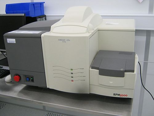
PhotoLuminescence Mapper RPM2000

This page is done by DTU Nanolab internal Photoluminescence mapping is a non-contact, non-destructive technique for mapping out uniformity of alloy composition, material quality and defects in substrates and of III-V epiwafers. The Rapid Photoluminiscence Mapper (RPM) is equipped with 3 lasers for PL measurements and a white-light source to map out thickness and reflectance of eg layers, microcavities and VCSELs.

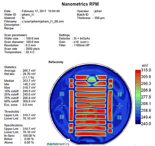
It can also be used to map out voids after silicon wafer-bonding. This is done using the reflectance mapping and is using the fact that silicon is transparent for wavelengths above ~1000nm. A void will therefor change the reflectance in that wavelength range. See datasheet below (Thanks to Jens Hemmingsen for the data).
The user manual and contact information can be found in LabManager:
PL mapper, Made by Jens Hemmingsen @ DTU Nanolab
| Performance | Excitation |
|
|---|---|---|
| Detection |
| |
| Gratings |
| |
| Chuck sizes |
| |
| Resolution |
| |
| Wavelength accuracy |
| |
| Materials | Allowed substrate materials |
|
| Forbidden materials |
| |
| Software | RPM viewer |
|
