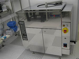
Specific Process Knowledge/Thin film deposition/ALD Picosun R200
ALD1
Feedback to this page: click here
ALD - Atomic layer deposition

The ALD1 (Picosun R200 ALD) tool is used to deposit a very thin layer of Al2O3, TiO2 (amorphous or anatase), HfO2, ZnO and AZO (Al-doped ZnO) on different samples.
Each process is using two (or three for AZO) different precursors. The reaction takes place in cycles. During each cycle, a very short pulse of each precursor is introduced into the ALD reaction chamber in turns, and in-between each precursor pulse the chamber is purged with nitrogen. All reactions have to take place on the sample surface, thus it is very important that each precursor is removed from the chamber before the next one is introduced. In that way, materials can be deposited atomic layer by atomic layer by ALD.
In order to ensure that the ALD reactor has the same temperature everywhere, it has a dual chamber structure. The inner chamber is the reactor chamber, and the outer chamber is a vacuum chamber that is isolating the reactor from room air. The space between the two chambers is called an intermediate space (IMS), and this is constantly purged with nitrogen. A sample holder is placed in the reactor chamber.
When the reactor chamber is heated up or cooled down, it will take some time before the sample holder and the sample reaches the desired temperature. Thus, it is important to include a temperature stabilization time in the process recipes.
The ALD deposition takes place in the reactor chamber. All precursor and nitrogen carrier gas lines are connected to the reactor chamber through separate gas lines. The precursor pulse time is controlled using special ALD valves, that allow very short precursors pulses to be introduced into the ALD reactor and at the same time allow a constant nitrogen purge.
The ALD reaction takes place under vacuum, thus a vacuum pump is connected to the bottom of the ALD reactor chamber. The pump is located in the basement.
The liquid precursors (H2O, TMA, TiCl4, DEZ and TEMAHf) are located in the cabinet below the ALD chamber. When these precursors are not in use, the manual valves have to be closed. Only four of the precursors (normally H2O, TMA, TEMAHf and either TiCl4 or DEZ) can be connected at the same time. Ozone is generated by use of an ozone generator that is located on the side of the machine.
It is possible to change the sample holder, so that ALD deposition can take place on different samples, e.g. a small wafer batch (up to five wafers at a time) or a number of smaller samples. Samples are loaded manually into the sample holder by use of a tweezer. However, for some materials the uniformity will only be good for the top sample(s) in a minibatch holder.
A short presentation with some information about the ALD tool can be found here.
The user manual, the user APV and contact information can be found in LabManager:
Process information
- Standard recipes on the ALD 1 tool
- Advanced recipes involving fabrication of multilayers
- Al2O3 deposition using ALD 1
- TiO2 deposition using ALD 1
- ZnO deposition using ALD 1
- Al-doped ZnO (AZO) deposition using ALD 1
- HfO2 deposition using ALD 1
| Equipment | ALD1 | |
|---|---|---|
| Purpose | ALD (atomic layer deposition) of |
|
| Performance | Deposition rates |
|
| Thickness |
| |
| Process parameter range | Temperature window |
|
| Precursors |
| |
| Substrates | Batch size |
|
| Allowed materials |
| |
