Specific Process Knowledge/Characterization/PL mapper

From LabAdviser
Revision as of 07:51, 22 August 2014 by Bghe (talk | contribs) (Created page with "'''Feedback to this page''': '''[mailto:danchipsupport@danchip.dtu.dk?Subject=Feed%20back%20from%20page%20http://labadviser.danchip.dtu.dk/index.php?title=Specific_Process_Kno...")
(diff) ← Older revision | Latest revision (diff) | Newer revision → (diff)

Feedback to this page: click here

PhotoLuminescense Mapper RPM2000

Photoluminiscense mapping is a non-contact, non-destructive technique for mapping out uniformity of alloy composition, material quality and defects in substrates and of III-V epiwafers. The Rapid Photoluminiscense Mapper (RPM) is equipped with 3 lasers for PL measurements and a white-light source to map out thickness and reflectance of eg layers, microcavities and VCSELs.


The user manual and contact information can be found in LabManager:
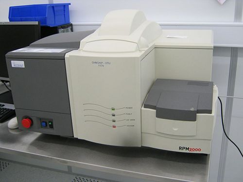
PL mapper


Positioned in the MOCVD room: F-1


Performance Excitation
  • ~100 mW @ 405 nm (~70mW on sample)
  • ~10 mW @ 532 nm
  • ~10 mW @ 980 nm
  • white light source for thickness and reflectance measurements
Detection
  • integrated signal: Si and/or InGaAs detector
  • Spectral scan: Si CCD (up to 1100 nm), InGaAs photodiode array (900-1700 nm)
Gratings
  • 600 lines/mm (single frame: 60 nm @ 400 nm)
  • 300 lines/mm (single frame: 120 nm @ 900 nm)
  • 150 lines/mm (single frame: 270 nm @ 1550 nm)
Chuck sizes
  • 2", 3" and 4"
Resolution
  • Minimum spatial resolution 100 µm
  • spotsize ~100 µm
Wavelength accuracy
  • < +/- 1 nm
Materials Allowed substrate materials
  • III-V
  • Silicon
Forbidden materials
  • Do not map any wafers that might leave residues in the machine
Software RPM viewer
  • Software (free) to view and re-analyse the maps and spectra can be found on Labmanager.
  • Direct link to file download RPM2000 analysis software.
  • The software will request you to get a (free) license key from Nanometrics.