Specific Process Knowledge/Thin film deposition/Deposition of Silicon Oxide/Deposition of Silicon Oxide using LPCVD TEOS
Feedback to this page: click here
LPCVD TEOS Furnace (B3)


Danchip have one LPCVD furnace for deposition of TEOS: The furnace was installed in 1995 and can handle 4" wafers. It is furthermore possible to dope the TEOS with Boron.
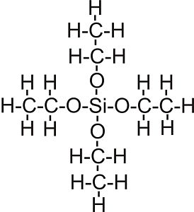
TEOS is Tetra-Ethyl-Ortho-Silicate, it is also sometimes referred to as Tetra-Ethoxy-Silane. The difference between TEOS and Silane is essentially that is TEOS the silicon atom is already oxidised. Therefore the conversion of TEOS to Silicon dioxide is a rearrangement rather than an oxidation. As can be seen from figure 1 what is basically required to deposit Silicon dioxide is a removal of two oxygen atoms for that a relative high temperature of 725 oC.
On the LPCVD TEOS furnace there are two standard processes for deposition, one for thin oxides called TEOSPNE and one for thicker oxides called TEOSSLOW. The only difference is that in the case of the TEOSSLOW recipe the furnace opens significantly slower. Thick TEOS layers have a tendency to form cracks if they are moved to fast out of the furnace.
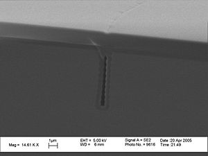
TEOS can be used as an alternative to thermally grown or PECVD oxide, it has a dielectric constant of 3.56 (For thermal oxide it is 3.46). Furthermore TEOS has a very high surface mobility enabling it to fill holes that has a large aspect ratio and leaving the surface quite smooth see figure 2, hence it also covers corners and side walls very well.
Process parameters for the two standard deposition recipes on the TEOS furnace:
| Recipe name | Wafer size and number of wafers | Temperature [oC] | Pressure [mTorr] | TEOS gas flow [sccm] | O gas flow [sccm] | PH gas flow [sccm] | TMB gas flow [sccm] | Comments |
|---|---|---|---|---|---|---|---|---|
| "TEOSPNE" | 4" wafers
1-17 wafers in a run |
725 | 190 | 50 | 30 | 0 | 0 | Standard TEOS recipe |
| "TEOSSLOW" | 4" wafers
1-17 wafers in a run |
725 | 190 | 50 | 30 | 0 | 0 | Recipe used for thick layers |
Deposition rate:
The deposition rate is normally a little over 10nm/min (10.5nm/min) and the refractive index is around 4.44 for both recipes.
Using LPCVD TEOS as a masking material for KOH etching
It is possible to use TEOS as a masking layer in KOH etch however it is not as suitable as Silicon nitride for deep KOH etching. However for shallower etches it can be used. In comparison to silicon nitride TEOS has the advantage that it does not have the same pinhole problems.
