Specific Process Knowledge/Characterization/SEM: Scanning Electron Microscopy


Scanning electron microscopy at Danchip
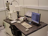
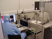
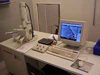
The four SEM's at Danchip cover a wide range of needs both in the cleanroom and outside: From the fast in-process verification of different process parameters such as etch rates, step coverages or lift-off quality to the ultra high resolution images on any type of sample intended for publication.
The 'workhorse' SEM that will cover most users needs is the Leo SEM. It is a very reliable and rugged instrument that provides high quality images of most samples. Excellent images on a large variety of materials such as semiconductors, semiconductor oxides or nitrides, metals, thin films and some polymers may be acquired on the Leo SEM. As such, we prefer that new users that have no prior SEM experience get trained on the Leo SEM before they start using the FEI or Zeiss.
The Zeiss SEM is the newest SEM in the cleanroom. It's a state-of-the-art SEM that will produce excellent images on almost any sample. Operated by the same user interface as the Leo, it is quite straight forward to change between the two instruments.
The FEI SEM is a versatile microscope with two vacuum modes (High Vacuum and Low Vacuum) and 6 different detectors, offering excellent resolution on any type of sample or material including graphene and carbon nanotubes. Somewhat more fragile compared to the robust Leo, it is our intention that only users with special needs (for instance thick polymers, glass substrates or EDX/micromanipulator experiments) that will be trained.
Outside the cleanroom in the basement of building 347, the Jeol SEM provides a possibilty of imaging samples that do not go into the cleanroom.
The user manuals, quality control procedures and results, user APVs, technical information and contact information can be found in LabManager:
Process information
| Equipment | SEM Leo | SEM Zeiss | SEM FEI | SEM Jeol | |
|---|---|---|---|---|---|
| Model | Leo 1550 SEM | Zeiss Supra 40 VP | FEI Nova 600 NanoSEM | Jeol JSM 5500 LV | |
| Purpose | Imaging |
|
|
|
|
| Performance | Resolution |
|
|
|
|
| Optimum usage |
|
|
|
| |
| Process parameter range | Detectors |
|
|
|
|
| Stage |
|
|
|
| |
| Electron source |
|
|
|
| |
| Operating pressures |
|
|
|
| |
| Substrates | Sample sizes |
|
|
|
|
| Allowed materials |
|
|
|
| |
| SEM - Zeiss | SEM - FEI | SEM - Leo | SEM - Jeol | |
|---|---|---|---|---|
| Model | Zeiss Supra 55 VP | FEI Nova 600 NanoSEM | Leo 1550 SEM | Jeol JSM 5500 LV SEM |
| Substrate size | Up to 6" wafer with full view | Up to 6" wafer with 4" full view | Up to 4" wafer with full view | |
| Additional equipment | Kleindiek micromanipulator with Capres 4 point probe | |||
| EDX analysis | Oxford Inca system | Röntec system | Not available |
