Specific Process Knowledge/Lithography/EBeamLithography/JEOL 9500 User Guide

Purpose, location and technical specifications
Type and location of machine
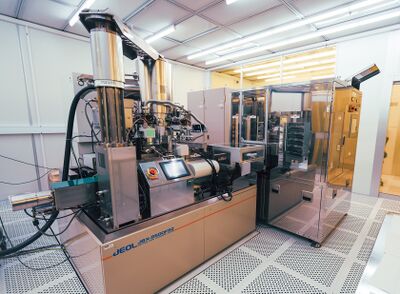
The JEOL JBX-9500FS electron beam lithography system is a spot electron beam lithography system designed for use in writing patterns (10 nm - 1 µm) in electron sensitive resists. The JEOL JBX-9500FS was purchased in 2012 and is installed in E-1 and E-2 at DTU Nanolab. The main console of the e-beam writer is installed in E-2 which is a class 10 (ISO 4) cleanroom with tight temperature and moisture control. The computer controlling the e-beam (EWS/9500) and the computer supporting the conversion of e-beam files are located in E-1 which is a class 100 (ISO 5) cleanroom.
Authorization
- Only authorized users are allowed to use this machine.
- In E-2, all users must keep within the area between the front side of the machine and the table with the pre-aligner setup. Only JEOL staff or DTU Nanolab staff may access the backside of the machine.
- No users, not even authorised users, are allowed to load a substrate into the automatic cassette transfer system.
- After your exposure, fully trained users can unload their cassettes from the automatic cassette transfer system and unmount their substrates.
- If you are unable to unmount your substrates before another user requires the cassette, you must accept that either the next user or DTU Nanolab personel unmount your substrates.
Original JEOL Manual
The original JEOL manual for the e-beam writer JEOL JBX-9500FS is located on the O-drive: O:\CleanroomDrive\_Equipment\E-beam
Techical Specification
The system can be characterized as follows:
- The spot beam for electron beam writing is generated by a ZrO/W emitter and a four-stage electron beam focusing lens system.
- The maximum frequency of the deflector scanner is 100 MHz, i.e. the minimum beam dwell time is 10 ns.
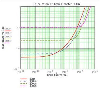
- The acceleration voltage is locked at 100 kV.
- The e-beam writer can pattern structures with a minimum resolution of 10 nm.
- The maximum writing field size is 1000 µm x 1000 µm.
- The machine has cassettes that can contain either 6 wafers of 2” in size, 2 or 3 wafers of 4” in size, 1 wafer of 6” in size, 1 wafer of 8” in size, 4 chips of different sizes(slot sizes 4 mm, 8 mm, 12 mm, and 20 mm). See the Cassette specification page for more information
Rough estimation of exposure time
Pattern writing using the e-beam writer is implemented on a wafer or chip which has been coated with an electron sensitive resist. Both positive and negative types of resists for pattern writing can be used. In either case, the resist sensitivity Q (C/cm2) is a function of the beam current, I (A), the pattern writing area, A (cm2), and the pattern writing time t (s), as given below:
Q = It/A
The e-beam scanning frequency f (Hz) is a function of the e-beam scanning step, p (shot step), as shown below:
f = I /(Qp2)
The e-beam writer has scan speeds up to 100 MHz available. The dose, Q, shot step, p, and current, I, is chosen to meet the requirement of the pattern to be written, the writing time available, and also to meet the requirement f < 100MHz.
Based on the equations above, a rough estimate of the exposure time is easily calcualted. In the second sheet of the e-beam logbook, a simple program for calculating the scan speed frequency and an estimation of the exposure time can be found. Note, that the actual writing time will exceed this estimated exposure-time, as the exposure-time calculation does not include pre-calibrations and stage movement during exposure.
The area of your pattern can easily be found in L-edit by selecting all of your structure and use the area calculator in Tools/Add-Ins. If your pattern contains instances, you have to flatten your pattern (Cell/Flatten) before you use the area calculator; notice, however, that the flattening cannot be undone.

