Specific Process Knowledge/Thin film deposition/Lesker
Film quality optimization
By Bjarke Thomas Dalslet @Nanotech.dtu.dk
The Lesker CMS 18 sputter system can produce films in a wide range of qualities. The quality of a film depends strongly on the substrate (lattice matching), but also on the energy the sputtered material can utilize for annealing.
Strain estimations was done on 30 nm NiFe thin films using low angle x-ray diffraction, for various substrates. It was found that the strain of the film influenced the resistance (R) and anisotropic magneto resistance (AMR) of the films (this relationship is also documented in literature); A Ta interface layer reduced R and increased AMR on both Si and SiO substrates while reducing strain.
This study was then done on 30 nm NiFe thin films deposited on 3 nm Ta on top of a SiO substrate, using R and AMR as an indication of strain. As seen in the tables, applying a substrate bias increases AMR and conductance (1/R). An equivalent effect is seen when heating the substrate during deposition. This heating can also be done after deposition without loosing the effect.
| Name | Substrate bias (W) | AMR | 1/R (S) | Crystal strain |
| 0029 NiFe3_stack_RF20 | 20 | 0.02724278 | 1.308044474 | |
| 0018_NiFe1_stack_RF | 10 | 0.025850358 | 0.898311175 | |
| 0030 NiFe3_stack | 0 | 0.020103598 | 0.71772052 | 0.8 |
| Name | Temperature (C) | AMR | 1/R (S) | Crystal strain |
| 0030 NiFe3_stack | 25 | 0.020103598 | 0.71772052 | 0.8 |
| BDT-NiFe1-blank30 | 200 | 0.019319002 | 1.095770327 | |
| BTD-NiFe-Blank22 | 250 | 0.021768497 | 1.047668937 | |
| BTD-NiFe-Blank14 | 300 | 0.02983617 | 1.724137931 | |
| BTD-NiFe-Blank13 | 350 | 0.033944331 | 1.887504719 | |
| BTD-NiFe-Blank15 | 400 | 0.031176801 | 1.655903295 | 0.2 |
| BTD-NiFe-Blank16 | 450 | 0.030843457 | ||
Surface roughness optimization
By Bjarke Thomas Dalslet @Nanotech.dtu.dk
The Lesker CMS 18 sputter system provides thin films of varying surface roughness. This rougness was verified to be dependent on the sputtered material, sputter mode (DC or RF) and the substrate bias strength. Other probable factors include sputter power and pressure. Below is a table for three cases.
The "From SiO target (RF sputter)" study was done on clean Si substrates. The sputter power was 157W and the pressure 3.5 mTorr using RF sputtering of a SiO target. The film thicknesses were around 42 nm.
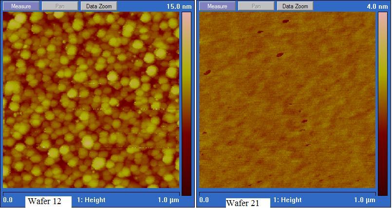
The "From Si target (DC sputter)" study was done on clean Si substrates. The sputter pressure 3 mTorr using DC reactive sputtering of a Si target. Oxygen was added to the argon sputter gas. Above 10% O the gun seems to oxidize (at this sputter power). The figure shows the difference in AFM images between no RF bias (wafer 12) and RF bias (Wafer 21)
The "Ta" study was done on clean Si substrates. The sputter pressure was 3 mTorr using DC sputtering of a Ta target. Some O was added to wafer 25 and 26 to make TaO. In order to get fully oxidized films, up to 30-45% O should be added. Consult the thesis of Carsten Christensen for details on TaO.
Other studies on metals (NiFe/MnIr) show only limited effect of the substrate bias on the roughness.
From SiO2 target (RF sputter)
| Wafer nr | RF bias (W) | Reactive O2 (%) | Power(W) | Rq (RMS) (nm) | Thickness |
| 3 | 0 | 0 | 157 | 0.902 | |
| 6 | 5 | 0 | 157 | 0.499 | 44 |
| 7 | 10 | 0 | 157 | 0.142 | 42 |
| 8 | 15 | 0 | 157 | 0.422 | 40 |
From Si target (DC sputter)
| Wafer nr | RF bias (W) | Reactive O2 (%) | Power(W) | Rq (RMS) (nm) | Thickness |
| 12 | 0 | 5 | 135 | 1.44 | 123 nm (ellipsometry) |
| 13 | 0 | 9 | 130 | 1.32 | 98 nm (ellipsometry) |
| 14 | 0 | 13 | 100 | 1.37 | 71.5 nm (ellipsometry) |
| 15 | 10 | 9 | 90 | 0.984 | 56.25 nm (ellipsometry) |
| 21 | 20 | 9 | 90 | 0.112 | |
| 22 | 15 | 9 | 90 | 0.509 |
Ta
| Wafer nr | RF bias (W) | Reactive O2 (%) | Power(W) | Rq (RMS) (nm) | Thickness |
| blank1 | 0 | 0 | 180 | 0.209 | |
| 16 | 10 | 0 | 180 | 0.36 | 56 |
| 24 | 20 | 0 | 180 | 0.357 | |
| 25 | 20 | 9 | 180 | 0.202 | 110 |
| 26 | 20 | 5 | 180 | 0.194 | 95 |
| 27 | 15 | 0 | 180 | 0.413 | |
| 28 | 25 | 0 | 180 | 0.164 | |
| 31 | 30 | 0 | 180 | 0.3 |

