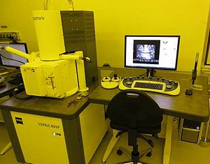
Specific Process Knowledge/Characterization/SEM Supra 3
Appearance
THIS PAGE IS UNDER CONSTRUCTION
Feedback to this page: click here

The user manuals, quality control procedures and results, user APVs, technical information and contact information can be found in LabManager:
SEM's at DTU Danchip:
- The SEM Leo page in LabManager,
- The SEM Supra 1 page in LabManager,
- The SEM Supra 2 page in LabManager,
- The SEM Supra 3 page in LabManager,
| Equipment | SEM Supra 2 (Supra 60VP SEM) | |
|---|---|---|
| Purpose | Imaging and measurement of |
|
| Location |
| |
| Performance | Resolution |
The resolution is strongly dependent on the type of sample and the skills of the operator. |
| Instrument specifics | Detectors |
|
| Stage |
| |
| Electron source |
| |
| Operating pressures |
| |
| Options |
| |
| Substrates | Batch size |
|
| Allowed materials |
| |
