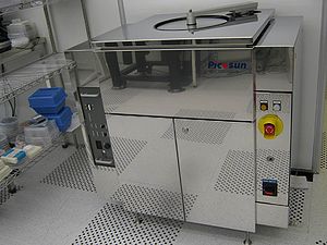
Specific Process Knowledge/Characterization/SEM LEO
THIS PAGE IS UNDER CONSTRUCTION
Feedback to this page: click here
SEM LEO

A Danchip there are five scanning electron microscopes (SEMs). These SEMs cover a wide range of needs both in the cleanroom and outside: From the fast in-process verification of different process parameters such as etch rates, step coverages or lift-off quality to the ultra high resolution images on any type of sample intended for publication.
The SEM LEO was installed in the cleanroom in the 1998, and the software was ungraded in 2012.
This SEM will cover most users need. It is a very reliable and rugged instrument that provides high quality images of most samples. Excellent images on a large variety of materials such as semiconductors, semiconductor oxides or nitrides, metals, thin films and some polymers may be acquired on the SEM.
The SEM is is equipped with a Raith e-beam writing system.
The user manual, control instruction, the user APV and contact information can be found in LabManager:
SEM LEO info page in LabManager,
Process information
- Standard recipes on the ALD tool
- Results from the ALD acceptance test
- Al2O3 deposition using ALD
- TiO2 deposition using ALD
| Equipment | ALD Picosun R200 | |
|---|---|---|
| Purpose | ALD (atomic layer deposition) of |
Please note that it might not be possible to deposit all marials at the same time |
| Performance | Deposition rates |
|
| Thickness |
| |
| Process parameter range | Temperature |
|
| Precursors |
Please note that not all precursors might be mounted on the tool at the same time | |
| Substrates | Batch size |
|
| Allowed materials |
| |
