Specific Process Knowledge/Characterization/Profiler
Feedback to this page: click here
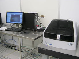
Dektak XTA_new stylus profiler
The newer Dektak XTA stylus profiler is usable for profiling surfaces of samples with structures in the micro- and nanometer range. A profil measurement can be done in a specific point by using a high magnification camera to locate the structure. It is also possible to program the stylus to measure in several positions, defined with respect to some deskew points. Stress measurements of thin films can be done by measuring the wafer bow.
A rough overview of the performance of Dektak XTA_new

| Purpose | Profiler for measuring micro structures. |
|
|---|---|---|
| Performance | Scan range x y |
Line scan x: 50 µm to 55 mm in a single scan, up to 200 mm with stiching |
| Scan range z |
50 Å to 1 mm | |
| Resolution xy |
down to 0.003 µm | |
| Resolution z |
1Å, 10Å, 80Å or 160Å (for ranges 65kÅ, 655 kÅ, 5240 kÅ and 1mm respectively) | |
| Max. scan depth as a function of trench width W |
1.2(W[µm]-5µm) | |
| Hardware settings | Tip radius |
|
| Substrates | Substrate size |
|
| Substrate material allowed |
|
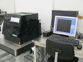
Dektak 8 stylus profiler

Dektak 8 stylus profiler is a product of Veeco Instruments. It is usable for profiling surfaces of samples with structures in the micrometer range. It can measure in a specific point found with help from high magnification video cameras or it can be programmed to measure several points defined with respect to some deskew points. It can also be used for stress measurements of thin films by measuring the wafer bow.
To get some product information and some tips and tricks from the vendor take a look at Veeco's homepage [1]
A rough overview of the performance of Dektak 8 stylus profiler
| Purpose | Profiler for measuring micro structures. |
|
|---|---|---|
| Performance | Scan range xy |
Line scan x: 50 µm to 100 mm |
| Scan range z |
50 Å to 1 mm | |
| Resolution xy |
down to 0.067 µm | |
| Resolution z |
1Å, 10Å, 40Å or 160Å (for ranges 65kÅ, 655 kÅ, 2620 kÅ and 1mm respectively) | |
| Max. scan depth as a function of trench width W |
1.2(W[µm]-5µm) | |
| Hardware settings | Tip radius |
|
| Performance | Substrate size |
|
| Substrate material allowed |
|
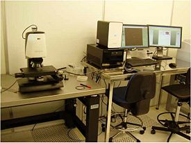
Optical Profiler (Sensofar)

The PLu Neox 3D Optical Profiler (from Sensofar) has a dual-technology sensor head that combines confocal and interferometry techniques as well as thick and thin film measurement capabilities.
The Neox sensor head provides standard microscope imaging, confocal imaging, confocal profiling, PSI (Phase Shift Interferometry), VSI (Vertical Scanning Interferometry) and high resolution thin film thickness measurements on a single instrument.
The main purpose is 3D topographic imaging of surfaces, step height measurements in smaller trenches/holes than can be obtained with standard stylus methods (i.e. with aspect ratios higher that 1:1), roughness measurements with larger FOV (Field Of View) than the AFM, but less horisontal resolution.
For most samples the optical profiler provides fast and easy information without any sample preparation. However, it can be necessary to cover thin transparent layers (< 2 µm) with a thin layer of metal.
The resolution is limited by the objectives and the pixel resolution. Also the depth of focus is limited, especially for higher magnifications.
The user manual, technical information and contact information can be found in LabManager:
Optical profiler (Sensofar) info page in LabManager
Process Information
| Equipment | Optical profiler | |
|---|---|---|
| Purpose | 3D topographic imaging of surfaces. |
|
| Posibilities | Confocal and interferometric profiling and reflectometry |
|
| Performance | Depending on the objective chosen | |
| Substrates | Substrate size |
|
| Substrate materials allowed |
| |
Comparing the profilers
Take a look at the topographic measurement page.

