Specific Process Knowledge/Etch/IBE⁄IBSD Ionfab 300/IBE Au etch
Appearance
Results from the acceptance test in February 2011
Acceptance test for Au etch:
| . | Acceptance Criteria |
Acceptance Results |
|---|---|---|
| Substrate information |
|
. |
| Material to be etched |
|
. |
| Mask information |
|
. |
| Features to be etched |
|
. |
| Etch depth |
|
|
| Etch rate |
|
|
| Etch rate uniformity |
|
|
| Reproducibility |
|
|
| Selectivity (Au etch rate/ZEP etch rate) |
|
|
| Etch profile |
|
|
Process parameters for the acceptance test
| Parameter | Au etch acceptance |
|---|---|
| Neutalizer current [mA] | 550 |
| RF Power [W] | 1300 |
| Beam current [mA] | 500 |
| Beam voltage [V] | 600 |
| Beam accelerator voltage | 400 |
| Ar flow to neutralizer [sccm] | 5.0 |
| Ar flow to beam [sccm] | 10.0 |
| Rotation speed [rpm] | 20 |
| Stage angle [degrees] | 30 |
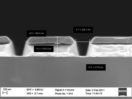
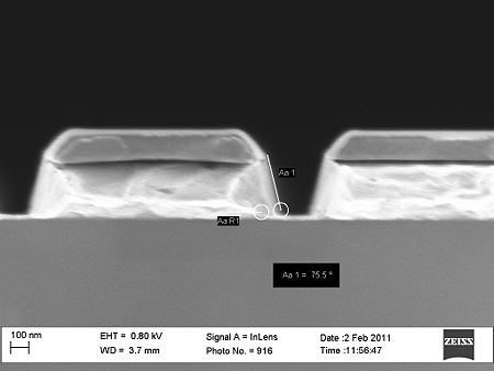
Some SEM profile images of the etched Au
 |
 |
|---|
IBE Au etch with Ti mask 
Work has been started to find a good process for etching gold with a Titanium mask with high selektivity.
| Ti etch test with Zep520A as mask - To etch the Ti mask | Au etch test with high selectivity to Ti | |
|---|---|---|
| Generel description | Generel description - method 1 | Generel description - method 2 |
| Recipe name |
test Ti acceptance 20111129 |
Au_acceptance_with_O2 |
| IBE parameters |
|
|
| Etch rate in resist |
12.8nm/min |
72nm/min |
| Etch rate in Au |
32.7nm/min |
42.6nm/min |
| Etch rate in Ti |
8.3nm/min |
4.3nm/min |
| Selectivity Ti/Zep |
0.65 |
0.06 |
| Selectivity Au/Ti |
3.9nm/min |
9.9nm/min |
