Specific Process Knowledge/Etch/Wet Silicon Nitride Etch: Difference between revisions
| Line 87: | Line 87: | ||
*Silicon oxides | *Silicon oxides | ||
|- | |- | ||
|} | |||
=<span style="background:#FF2800">THIS PAGE IS UNDER CONSTRUCTION</span>[[image:Under_construction.png|200px]]= | |||
=When a section is under construction - add this image next to the section headline: [[Image:section under construction.jpg|70px]]= | |||
==Comparison of Platinum Etch Methods== | |||
{|border="1" cellspacing="1" cellpadding="3" style="text-align:left;" | |||
|- | |||
|- | |||
|-style="background:silver; color:black" | |||
! | |||
![[Specific Process Knowledge/Etch/Wet Platinum Etch|Pt wet etch]] | |||
![[Specific_Process_Knowledge/Etch/IBE⁄IBSD Ionfab 300|IBE (Ionfab300+)]] | |||
|- | |||
|- | |||
|-style="background:WhiteSmoke; color:black" | |||
!Generel description | |||
|Wet etch of Pt | |||
|Sputtering of Pt | |||
|- | |||
|- | |||
|-style="background:LightGrey; color:black" | |||
!Etch rate range | |||
| | |||
*~?nm/min | |||
| | |||
*~30nm/min (not tested yet) | |||
|- | |||
|- | |||
|-style="background:WhiteSmoke; color:black" | |||
!Etch profile | |||
| | |||
*Isotropic | |||
| | |||
*Anisotropic (angles sidewalls, typical around 70 dg) | |||
|- | |||
|-style="background:LightGrey; color:black" | |||
!Masking material | |||
| | |||
*None (only used for stripping Pt) | |||
| | |||
*Any material that is allowed in the chamber, photoresists included | |||
|- | |||
|- | |||
|-style="background:WhiteSmoke; color:black" | |||
!Substrate size | |||
| | |||
*Any size and number that can go inside the beaker in use | |||
| | |||
Smaller pieces glued to carrier wafer | |||
*<nowiki>#</nowiki>1 50mm wafer | |||
*<nowiki>#</nowiki>1 100mm wafer | |||
*<nowiki>#</nowiki>1 150mm wafer | |||
*<nowiki>#</nowiki>1 200mm wafer | |||
|- | |||
|- | |||
|-style="background:LightGrey; color:black" | |||
!'''Allowed materials''' | |||
| | |||
No restrictions cross contamination wise as long as you use the right beaker and make sure that they are safe to enter in the chemicals | |||
| | |||
*Silicon | |||
*Silicon oxides | |||
*Silicon nitrides | |||
*Metals from the +list | |||
*Metals from the -list | |||
*Alloys from the above list | |||
*Stainless steel | |||
*Glass | |||
*III-V materials | |||
*Resists | |||
*Polymers | |||
*Capton tape | |||
|- | |||
|} | |} | ||
Revision as of 11:15, 30 May 2013
Feedback to this page: click here
Wet Silicon Nitride Etch

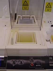
Wet Etching of silicon nitride - stoichiometric and Si-rich - is done in a dedicated laminar flow bench with an integrated quartz tank (Tiger Tank - TT-4). The quartz tank can take up to one 6" wafer carrier. The flow bench is placed in cleanroom 4. The process is mainly used to strip silicon nitride (maskless), but can also be used for masked etching of silicon nitride using some kind of silicon oxide as etch mask. However, the wet silicon nitride etch is isotropic - meaning that the under-etching (etch-bias) at least amounts to the thickness of the silicon nitride layer.
The etch solution is initially 85 wt% H3PO4 which is heated up to the boiling temperature - ca. 157 oC. Water is allowed to boil off thus raising the concentration and the boiling temperature of the solution until a boiling temperature of 180 oC is reached. Thereafter, the wafers are submerged into the bath and the water-cooled lid is closed to maintain the concentration and the boiling temperature. In some cases a lower boiling temperature is chosen - typically 160 oC - which lowers the etch rate and improves the selectivity RSi3N4 / RSiO2.
NB: Great care has to be taken in this process due to risk of "shock-boiling"
Nitride Etch data
| Nitride Etch @ 180 oC | Nitride Etch @ 160 oC | |
|---|---|---|
| General description |
Etch/strip of silicon nitride |
Etch/strip of silicon nitride |
| Link to safety APV and KBA | see APV here | see APV here |
| Chemical solution | H3PO4 (85 wt%) | H3PO4 (85 wt%) |
| Process temperature | 180 oC | 160 oC |
| Possible masking materials |
|
|
| Etch rate |
|
|
| Selectivity RSi3N4 / RSiO2 | ~20 | The selectivity (sirich nitride:oxide) is higher at 160 oC than at 180 oC |
| Batch size |
1-25 wafers at a time |
1-25 wafer at a time |
| Size of substrate |
2-6" wafers |
2-6" wafers |
| Allowed materials |
|
|
THIS PAGE IS UNDER CONSTRUCTION
When a section is under construction - add this image next to the section headline: 
Comparison of Platinum Etch Methods
| Pt wet etch | IBE (Ionfab300+) | |
|---|---|---|
| Generel description | Wet etch of Pt | Sputtering of Pt |
| Etch rate range |
|
|
| Etch profile |
|
|
| Masking material |
|
|
| Substrate size |
|
Smaller pieces glued to carrier wafer
|
| Allowed materials |
No restrictions cross contamination wise as long as you use the right beaker and make sure that they are safe to enter in the chemicals |
|
