Specific Process Knowledge/Etch/IBE⁄IBSD Ionfab 300/IBE Si etch: Difference between revisions
| Line 56: | Line 56: | ||
{| border="1" cellspacing="1" cellpadding="2" | {| border="1" cellspacing="1" cellpadding="2" | ||
! | ! | ||
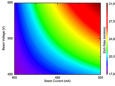
[[image:IBE-Si-ER-contour.jpg|400x400px|thumb|center| | [[image:IBE-Si-ER-contour.jpg|400x400px|thumb|center|IBE etch rate only shows a dependency on Beam Current and Beam Voltage. Values found on the plot should always be tested before use.]] | ||
! | ! | ||
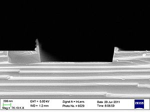
[[image:IBE-Si-CA-contour.jpg|400x400px|thumb|center|Silicon etch in IBE with rounded corners. Large hare ears with ripling are seen at the structure edge.]] | [[image:IBE-Si-CA-contour.jpg|400x400px|thumb|center|Silicon etch in IBE with rounded corners. Large hare ears with ripling are seen at the structure edge.]] | ||
|} | |} | ||
Revision as of 10:01, 10 December 2012
Results for Si etching in the IBE
Made by Kristian Hagsted Rasmussen @ Nanotech <br\>
Best recipe with respect to the etch profile and low redeposition:
| Parameter | Best Si etching recipe so fare |
|---|---|
| Neutalizer current [mA] | 450 |
| RF Power [W] | 1200 |
| Beam current [mA] | 400 |
| Beam voltage [V] | 600 |
| Beam accelerator voltage | 400 |
| Ar flow to neutralizer [sccm] | 6.0 |
| Ar flow to beam [sccm] | 6.0 |
| Rotation speed [rpm] | 20 |
| Stage angle [degrees] | 5 |
| Results | vvv |
| Etch rate [nm/min] | 17-18 |
Etch results
Some SEM profile images of the etched stacks
The silicon etch test was made as a preliminary test of the IBE system, to obtain a felling of the system capabilities and the different parameters influence on the etch outcome. A throughout characterization of the wafers was not carried out. However, the most important results are listed here. The table list the best etch definition obtained. The IBE etcher should only be used for silicon etching, if you have a specific need that cannot be accommodated in a RIE tool. This could be excessive amount of metals on the surface or a layer of silicon in a stack of several layers that all must be etched. The corner definition is strongly dependent on both accelerator and beam voltage and of course the incident angle. However, no interactions between parameters seem to influence the angle outcome. The good corner definition will introduce hare ears at the resist edge. Which is best limited by use of thin resist layers slightly thicker than needed to mask for the duration of the etch. Be aware that the selectivity between silicon and resist is poor.


