Specific Process Knowledge/Thermal Process/BCB Curing Oven: Difference between revisions
Appearance
| Line 22: | Line 22: | ||
!colspan="2" border="none" style="background:silver; color:black;" align="center"|Equipment | !colspan="2" border="none" style="background:silver; color:black;" align="center"|Equipment | ||
|style="background:WhiteSmoke; color:black"|<b> | |style="background:WhiteSmoke; color:black"|<b>BCB Curing Oven</b> | ||
|- | |- | ||
!style="background:silver; color:black;" align="center"|Purpose | !style="background:silver; color:black;" align="center"|Purpose | ||
| Line 46: | Line 46: | ||
*One 100 mm wafer | *One 100 mm wafer | ||
|- | |- | ||
| style="background:LightGrey; color:black"|Allowed materials | | style="background:LightGrey; color:black"|Allowed materials | ||
'''Use the right carrier wafer''' | |||
|style="background:WhiteSmoke; color:black"| | |style="background:WhiteSmoke; color:black"| | ||
*BCB | *BCB | ||
*III-V materials | |||
*Co-polymer | *Co-polymer | ||
*Silicon | *Silicon, silicon oxide, silicon nitride | ||
*Quartz | *Quartz | ||
*Resist (prebaked) | *Resist (prebaked) | ||
*Metal (only Al, Ni, Ge and Au) | |||
*Metal (only | |||
|- | |- | ||
|} | |} | ||
Revision as of 10:58, 3 December 2012
This page is under contruction
BCB Curing Oven
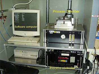
The BCB Curing Oven is mainly used for curing of BCB (bisbenzocyclobutene) and for alloying of metal in a nitrogen atmosphere.
During processing the furnace is rapidly heated by use of five halogen lamps below the sample. The furnace is purged with a high or a low nitrogen flow. Samples are processed at atmospheric pressure or at vacuum
The user manual, user APV, technical information and contact information can be found in LabManager:

Process information
There are no standard processes on the furnace.
| Equipment | BCB Curing Oven | |
|---|---|---|
| Purpose |
| |
| Process parameter range | Temperature |
|
| Nitrogen flows |
| |
| Substrates | Batch size |
|
| Allowed materials
Use the right carrier wafer |
| |
