Specific Process Knowledge/Characterization/Four-Point Probe: Difference between revisions
Appearance
| Line 16: | Line 16: | ||
!style="background:silver; color:black;" align="center"|Purpose | !style="background:silver; color:black;" align="center"|Purpose | ||
|style="background:LightGrey; color:black"| | |style="background:LightGrey; color:black"| | ||
|style="background:WhiteSmoke; color:black"| | |style="background:WhiteSmoke; color:black"| Resistance and resistivity measurement | ||
|- | |- | ||
| Line 24: | Line 24: | ||
Look at the process knowlege | Look at the process knowlege | ||
|- | |- | ||
!style="background:silver; color:black" align="center" valign="center" rowspan=" | !style="background:silver; color:black" align="center" valign="center" rowspan="2"|Process parameter range | ||
|style="background:LightGrey; color:black"|Process Temperature | |style="background:LightGrey; color:black"|Process Temperature | ||
|style="background:WhiteSmoke; color:black"| | |style="background:WhiteSmoke; color:black"| | ||
* | *room temperature | ||
|- | |- | ||
|style="background:LightGrey; color:black"|Process pressure | |style="background:LightGrey; color:black"|Process pressure | ||
|style="background:WhiteSmoke; color:black"| | |style="background:WhiteSmoke; color:black"| | ||
*1 atm | *1 atm | ||
|- | |- | ||
!style="background:silver; color:black" align="center" valign="center" rowspan="2"|Substrates | !style="background:silver; color:black" align="center" valign="center" rowspan="2"|Substrates | ||
|style="background:LightGrey; color:black"|Batch size | |style="background:LightGrey; color:black"|Batch size | ||
|style="background:WhiteSmoke; color:black"| | |style="background:WhiteSmoke; color:black"| | ||
*1 | *1 4" wafer per measurement | ||
|- | |- | ||
| style="background:LightGrey; color:black"|Substrate material allowed | | style="background:LightGrey; color:black"|Substrate material allowed | ||
|style="background:WhiteSmoke; color:black"| | |style="background:WhiteSmoke; color:black"| | ||
*Silicon wafers (new from the box or RCA cleaned) | *Silicon wafers (new from the box or RCA cleaned) | ||
|- | |- | ||
|} | |} | ||
Revision as of 12:04, 29 November 2012
Four-Point Probe
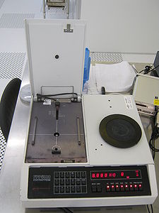
The Four-Point Probe is a Veeco FPP-5000 for I/V measurement. The main purpose it to measure resistance and resistivity on a 4" silicon wafer. But can also be used to find thickness of thin layers or test if is a N- or P-type wafer.
The wafer are pushed down on the four pins so a measurement is performed. It works only for 4" wafers because a special holder is need.

The user manual,technical information and contact information can be found in LabManager:
| Purpose | Resistance and resistivity measurement | |
|---|---|---|
| Performance |
Look at the process knowlege | |
| Process parameter range | Process Temperature |
|
| Process pressure |
| |
| Substrates | Batch size |
|
| Substrate material allowed |
|
