Specific Process Knowledge/Thermal Process/C3 Anneal-bond furnace: Difference between revisions
Appearance
| Line 1: | Line 1: | ||
==C3 Furnace Anneal Bond== | ==C3 Furnace Anneal Bond== | ||
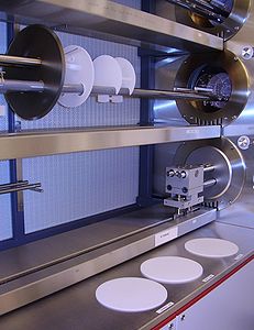
[[Image: | [[Image:C3.JPG|thumb|300x300px|C2 Furnace Anneal Bond: positioned in cleanroom 2]] | ||
C3 Furnace Anneal Bond is a Tempress horizontal furnace for oxidation and annealing of silicon wafers. | C3 Furnace Anneal Bond is a Tempress horizontal furnace for oxidation and annealing of silicon wafers. | ||
This furnace is the | This furnace is the third furnace tube in the furnace C-stack positioned in cleanroom 2. In this furnace it is allowed to enter wafers that comes directly from bonding in EVG NIL (assuming they were very clean when entering EVG NIL). Check the [http://www.labmanager.danchip.dtu.dk/view_binary.php?fileId=1250 cross contamination chart]. If you are in doubt, please send a mail to [mailto:furnace@danchip.dtu.dk furnace@danchip.dtu.dk]. | ||
'''The user manual(s), technical information and contact information can be found in LabManager:''' | |||
'''[http://www.labmanager.danchip.dtu.dk/function.php?module=Machine&view=view&mach=89 Anneal Bond]''' | |||
==Process knowledge== | ==Process knowledge== | ||
Revision as of 15:33, 26 November 2012
C3 Furnace Anneal Bond

C3 Furnace Anneal Bond is a Tempress horizontal furnace for oxidation and annealing of silicon wafers.
This furnace is the third furnace tube in the furnace C-stack positioned in cleanroom 2. In this furnace it is allowed to enter wafers that comes directly from bonding in EVG NIL (assuming they were very clean when entering EVG NIL). Check the cross contamination chart. If you are in doubt, please send a mail to furnace@danchip.dtu.dk.
The user manual(s), technical information and contact information can be found in LabManager:
Process knowledge
| Purpose | Oxidation and annealing | Oxidation:
|
|---|---|---|
| Performance | Film thickness |
|
| Process parameter range | Process Temperature |
|
| Process pressure |
| |
| Gas flows |
| |
| Substrates | Batch size |
|
| Substrate material allowed |
|
