Specific Process Knowledge/Etch/IBE⁄IBSD Ionfab 300/IBE magnetic stack etch: Difference between revisions
Appearance
| Line 40: | Line 40: | ||
|} | |} | ||
===Some SEM profile images of the etched | ===Some SEM profile images of the etched stacks=== | ||
{| border="1" cellspacing="1" cellpadding="2" | {| border="1" cellspacing="1" cellpadding="2" | ||
! | ! | ||
| Line 46: | Line 46: | ||
! | ! | ||
[[image:IBE magnetic stack A16-13.jpg|300x300px|thumb|center|]] | [[image:IBE magnetic stack A16-13.jpg|300x300px|thumb|center|]] | ||
|- | |||
[[image:IBE magnetic stack A3-13.jpg|300x300px|thumb|center|]] | [[image:IBE magnetic stack A3-13.jpg|300x300px|thumb|center|]] | ||
|} | |} | ||
Revision as of 15:05, 27 September 2012
End point detection is achieved by SIMS, and the etch rate is approximately 25 Nm/min. Resist stripping can be hard due to burned resist, to remedy this try to lover the current; this will though chance the sidewall angle. For help, discussion and further info please contact Kristian Hagsted Rasmussen.
Results from the acceptance test in February 2011
Process parameters for the acceptance test
| Parameter | Ti etch acceptance |
|---|---|
| Neutalizer current [mA] | 450 |
| RF Power [W] | 800 |
| Beam current [mA] | 400 |
| Beam voltage [V] | 500 |
| Beam accelerator voltage | 500 |
| Ar flow to neutralizer [sccm] | 5.0 |
| Ar flow to beam [sccm] | 10.0 |
| Rotation speed [rpm] | 20 |
| Stage angle [degrees] | 5 |
| Helium backside cooling [Torr] | 37.5 |
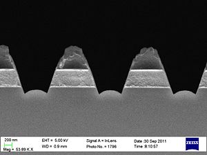
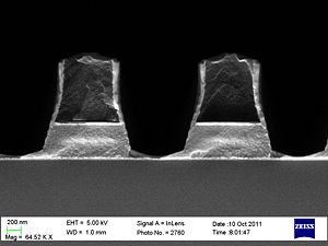
Some SEM profile images of the etched stacks

 |
 |
|---|
