Specific Process Knowledge/Etch/IBE⁄IBSD Ionfab 300/IBE magnetic stack etch: Difference between revisions
Appearance
New page: End point detection is achieved by SIMS, and the etch rate is approximately 25 Nm/min. Resist stripping can be hard due to burned resist, to remedy this try to lover the current; this will... |
No edit summary |
||
| Line 1: | Line 1: | ||
End point detection is achieved by SIMS, and the etch rate is approximately 25 Nm/min. | End point detection is achieved by SIMS, and the etch rate is approximately 25 Nm/min. | ||
Resist stripping can be hard due to burned resist, to remedy this try to lover the current; this will though chance the sidewall angle. For help, discussion and further info please contact Kristian Hagsted Rasmussen. | Resist stripping can be hard due to burned resist, to remedy this try to lover the current; this will though chance the sidewall angle. For help, discussion and further info please contact Kristian Hagsted Rasmussen. | ||
==Results from the acceptance test in February 2011== | |||
'''Acceptance test for Ti etch:''' | |||
{| border="2" cellspacing="0" cellpadding="2" | |||
|- | |||
!style="background:silver; color:black;" align="left"|. | |||
|style="background:WhiteSmoke; color:black"|'''Acceptance Criteria''' | |||
| | |||
'''Acceptance Results''' | |||
|- | |||
!style="background:silver; color:black;" align="left"|Substrate information | |||
|style="background:WhiteSmoke; color:black"| | |||
*50 mm SSP Si wafer | |||
*525 µm thick | |||
*Supplied by Danchip | |||
|. | |||
|- | |||
!style="background:silver; color:black" align="left" valign="top" |Material to be etched | |||
|style="background:WhiteSmoke; color:black"| | |||
*E-beam deposited Ti | |||
|. | |||
|- | |||
!style="background:silver; color:black" align="left" valign="top" rowspan="1"|Mask information | |||
|style="background:WhiteSmoke; color:black"| | |||
*E-beam resist mask: | |||
# 400nm of spin coated ZEP520A e-beam resist | |||
#Patterned by E-beam lithography | |||
|. | |||
|- | |||
!style="background:silver; color:black" align="left" valign="top"|Features to be etched | |||
|style="background:WhiteSmoke; color:black"| | |||
*300nm - 3µm dots and lines + a square of 200µmx200µm | |||
|. | |||
|- | |||
!style="background:silver; color:black" align="left" valign="top"|Etch depth | |||
|style="background:WhiteSmoke; color:black"| | |||
*300nm | |||
| | |||
*~270 nm | |||
|- | |||
!style="background:silver; color:black" align="left" valign="top"|Etch rate | |||
|style="background:WhiteSmoke; color:black"| | |||
*>80nm/min | |||
| | |||
*22nm/min +- 0.3nm/min (one standard deviation) | |||
|- | |||
!style="background:silver; color:black" align="left" valign="top"|Etch rate uniformity | |||
|style="background:WhiteSmoke; color:black"| | |||
*<+-2% | |||
| | |||
*+-(0.2% +-0.2%) | |||
|- | |||
!style="background:silver; color:black" align="left" valign="top"|Reproducibility | |||
|style="background:WhiteSmoke; color:black"| | |||
*<+-2% | |||
| | |||
*+-(0.8% +-0.5%) | |||
|- | |||
!style="background:silver; color:black" align="left" valign="top"|Selectivity (Au etch rate/ZEP etch rate) | |||
|style="background:WhiteSmoke; color:black"| | |||
*At least 1:1 | |||
| | |||
*0.7:1 | |||
|- | |||
!style="background:silver; color:black" align="left" valign="top"|Etch profile | |||
|style="background:WhiteSmoke; color:black"| | |||
*70-90dg. | |||
| | |||
*~65dg @270nm | |||
*~77dg @123nm | |||
|} | |||
====Process parameters for the acceptance test==== | |||
{| border="2" cellspacing="2" cellpadding="3" | |||
!Parameter | |||
!Ti etch acceptance | |||
|- | |||
|Neutalizer current [mA] | |||
|550 | |||
|- | |||
|RF Power [W] | |||
|1200 | |||
|- | |||
|Beam current [mA] | |||
|500 | |||
|- | |||
|Beam voltage [V] | |||
|600 | |||
|- | |||
|Beam accelerator voltage | |||
|400 | |||
|- | |||
|Ar flow to neutralizer [sccm] | |||
|6.0 | |||
|- | |||
|Ar flow to beam [sccm] | |||
|6.0 | |||
|- | |||
|Rotation speed [rpm] | |||
|20 | |||
|- | |||
|Stage angle [degrees] | |||
|20 | |||
|- | |||
|} | |||
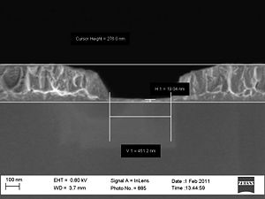
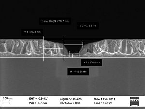
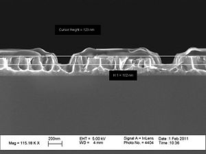
===Some SEM profile images of the etched Ti=== | |||
{| border="1" cellspacing="1" cellpadding="2" | |||
! | |||
[[image:IBE acceptance Ti S10-4.jpg|300x300px|thumb|center|Ti s10-4: 270nm deep - 500nm line. all zep has gone. Profile: ~65 dg.]] | |||
! | |||
[[image:IBE acceptance Ti S10-5.jpg|300x300px|thumb|center|Ti s10-5: 270nm deep - 300nm line. All zep has gone. Profile: ~65 dg.]] | |||
! | |||
[[image:IBE acceptance Ti S7 5.jpg|300x300px|thumb|center|Ti S7 5: 123nm deep - 300nm line. Still zep left. Profile: ~77 dg ]] | |||
|} | |||
Revision as of 12:39, 27 September 2012
End point detection is achieved by SIMS, and the etch rate is approximately 25 Nm/min. Resist stripping can be hard due to burned resist, to remedy this try to lover the current; this will though chance the sidewall angle. For help, discussion and further info please contact Kristian Hagsted Rasmussen.
Results from the acceptance test in February 2011
Acceptance test for Ti etch:
| . | Acceptance Criteria |
Acceptance Results |
|---|---|---|
| Substrate information |
|
. |
| Material to be etched |
|
. |
| Mask information |
|
. |
| Features to be etched |
|
. |
| Etch depth |
|
|
| Etch rate |
|
|
| Etch rate uniformity |
|
|
| Reproducibility |
|
|
| Selectivity (Au etch rate/ZEP etch rate) |
|
|
| Etch profile |
|
|
Process parameters for the acceptance test
| Parameter | Ti etch acceptance |
|---|---|
| Neutalizer current [mA] | 550 |
| RF Power [W] | 1200 |
| Beam current [mA] | 500 |
| Beam voltage [V] | 600 |
| Beam accelerator voltage | 400 |
| Ar flow to neutralizer [sccm] | 6.0 |
| Ar flow to beam [sccm] | 6.0 |
| Rotation speed [rpm] | 20 |
| Stage angle [degrees] | 20 |


