Specific Process Knowledge/Characterization/Profiler/Optical Profiler (Sensofar) acceptance test: Difference between revisions
| Line 179: | Line 179: | ||
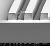
Measurement: Step height of patterned thick (10 µm) oxide on top of a silicon wafer.The pattern is aprox. 7µm thick | Measurement: Step height of patterned thick (10 µm) oxide on top of a silicon wafer.The pattern is aprox. 7µm thick | ||
Acceptance criteria: Step height must be within ±3% of a SEM profile measurement. See the SEM profile here: | Acceptance criteria: Step height must be within ±3% of a SEM profile measurement. See the SEM profile here: | ||
{| border="1" cellspacing="1" cellpadding="2" | |||
! | |||
[[Image:Sensofar_A5_SEM.pdf|100x100px|thumb|center|A1]] | |||
|} | |||
See the results here: | |||
{| border="1" cellspacing="1" cellpadding="2" | {| border="1" cellspacing="1" cellpadding="2" | ||
! | ! | ||
[[Media:Sensofar_A5_50xDI.pdf|100x100px|thumb|center|A1]] | [[Media:Sensofar_A5_50xDI.pdf|100x100px|thumb|center|A1]] | ||
|} | |} | ||
Revision as of 09:22, 24 August 2012
Results from the Optical Profiler (Sensofar) acceptance test
The acceptance test was performed in January 2012 by STInstruments and Sensofar together with Pernille V. Larsen @ Danchip and Berit G. Herstrøm @ Danchip.
This Table shows the acceptance criteria
| ' | Title | Sample description / measurement | Acceptance criteria |
| 1 | Patterned flat sample of silicon | Sample material: Patterned silicon substrate. | Depth 100±2 µm |
| Trench depth with aspect ratio 1:10 on a 10 µm wide trench | |||
| 2 | Patterned flat sample of silicon. | Sample material: Patterned silicon substrate. | Depth 91±2 µm |
| Trench depth with aspect ratio 1:11 on a 8 µm wide trench | |||
| 3 | Patterned flat sample of silicon | Sample material: Patterned silicon substrate | Depth 85±2 µm |
| Trench depth with aspect ratio 1:13 on a 6.4 µm wide trench | |||
| 4 | Patterned flat sample of glass | 3D profile of pattern etched down in a quartz sample. | Depth within ±1% from a standard profiler measurement and repeatability (3 successive measurements) within 0.1% |
| Pattern size 20 µm x 20 µm, depth 500 nm | |||
| 5 | Flat sample of silicon with thick patterned oxide | Step height of patterned thick (10 µm) oxide on top of a silicon wafer. | Step height must be within ±3% of a SEM profile measurement. |
| 7 µm deep pattern, trench width 6 µm | |||
| 6 | Flat sample of silicon with thick layer of patterned polymer | Sample material: SU8 on silicon. | Height 69±2 µm |
| Pillar heights of 69 µm with 25 µm between pillar edges | |||
| 7 | Free standing structure | Measure bow due to stress of a membrane. | Membrane bow repeatability of 5 successive measurement within 2% |
| Membrane material: Si(2 µm)/SiO2(~1 µm)/Au(50 nm). | |||
| Membrane size: honey comb structure approximately 150 µm in diameter. | |||
| Bow < 500 nm | |||
| 8 | Stitching of large area | Stitching 4 mm x 4 mm on same sample as in 7. The area consists of many closed packed honey comb formed membranes. | Membrane bow must the same as on 7 within 2% |
| 9 | Narrow trenches and holes | Sample material: Patterned silicon substrate. | Depth 20±2 µm |
| 2.5 µm wide trench in silicon with a depth of 20 µm | |||
| 10 | Film thickness measurement of transparent thin film | Transparent thin film thickness of 28 nm SiO2 on Si | SiO2 thickness 28±1 nm |
| 11 | Measurements of multiple stacks | 120 nm nitride on 110 nm oxide on a silicon substrate | Within ±2% on each layer from an ellipsometer measurement. |
| 12 | Film thickness measurements of transparent films on small structure | Sample material: Si with 1.5 µm patterned AZ-resist | Within ±1% from a standard profiler measurement. |
| Measure thickness of AZ-resist on pillars of 50 µm in diameter | |||
| 13 | Roughness repeatability | Sample material: Si wafer with poly-silicon layer. | Repeatability within 0.2% |
| 3 successive measurements of the roughness |
Results of acceptance test no. 1, 2 and 3
Sample material: Patterned silicon substrate Measurement: Trench depth with aspect ratio 1:10, 1:11 and 1:13 on a 10µm, 8mm and 6.4µm wide trenches respectively Acceptance criteria:Depth 100±2 µm, 91±2µm and 85±2µm. The SEM profile images of the three trenches are shown here:
 |
 |
 |
|---|
Test no. 1 was done in two ways:
- With confocal objective EPI 100x-N: See the results here
- With Interferometric objective 50X DI: See the results here
Test no. 2 was done using: confocal objective EPI 100x-N: See the results here
Test no. 3 was done using: confocal objective EPI 100x-N: See the results here
Setting for methode no. 1 for test no. 1,2 and 3: confocal
Recipe: Trench
- Operation mode: trench
- + Raw smoothing confocal
- + fine shift
- Objective: EPI 100X-N
- Z scan
- Dual - bottom up
- top: 8µm
- Gap: 91µm (the trench depth)
- Bottom: 8µm
- Speed factor: 1x
- + Linear stage
- Dual - bottom up
- Threshold: 0.0%
- Light source
- Levels: 2
- 900 -> 60 (might need to be set a little different)
- Gain: default
- Levels: 2
Setting for methode no. 2 for test no. 1: interferometric
We do not have a recipe for that but we used:
- Objective: Interferometric 50x DI
- Z scan: VSI
- Light souce: increased gain and contrast
Results of acceptance test no. 4
Sample material: Patterned fused silica.
Measurement: Depth of pattern
Standard profiler measurement:335nm
Acceptance criteria:Depth within ±1% from a standard profiler measurement (331.65nm-338.35nm) and repeatability (3 successive measurements) within 0.1%
It was done using interferometric measurements:
Objective: DI 50x-N
VSI z scan: 10µm
Treshold: 1%
Results
It was repeated 10 Time.
The first measurement is shown here
This table show the depth value for the 10 measurements
| ' | Measured depth [nm] |
| 1 | 337.5 |
| 2 | 336.5 |
| 3 | 334.7 |
| 4 | 335.5 |
| 5 | 339.2 |
| 6 | 337.2 |
| 7 | 334.2 |
| 8 | 335.5 |
| 9 | 341.1 |
| 10 | 344.4 |
| Average depth | 336.58 |
| Repeatability | 3% (the bad repeatability was accepted due to the high noise level in the room) |
Results of acceptance test no. 5
Sample: Flat sample of silicon with thick patterned oxide. Measurement: Step height of patterned thick (10 µm) oxide on top of a silicon wafer.The pattern is aprox. 7µm thick Acceptance criteria: Step height must be within ±3% of a SEM profile measurement. See the SEM profile here:
 |
|---|
See the results here: