Specific Process Knowledge/Characterization/XPS: Difference between revisions
No edit summary |
|||
| Line 52: | Line 52: | ||
The core electrons of the atoms are affected, meaning that the binding energy of the electrons are slightly shifted, when an atom is bonded to atoms of other elements. | The core electrons of the atoms are affected, meaning that the binding energy of the electrons are slightly shifted, when an atom is bonded to atoms of other elements. | ||
This gives an excelent tool for examining the chemistry of a surfaces, and how it is affected by different surface treatments. | This gives an excelent tool for examining the chemistry of a surfaces, and how it is affected by different surface treatments. | ||
If you study polymers, you can detect the precense of different chemical groups, for example (C-C),(C-OH),(C=O),(CF3) or (CF2-CH2) in the polymeric layer. And after surface treatments, you may examine differences in the polymeric layer. | |||
===Depth profiling=== | ===Depth profiling=== | ||
Revision as of 11:26, 24 October 2011
XPS-ThermoScientific

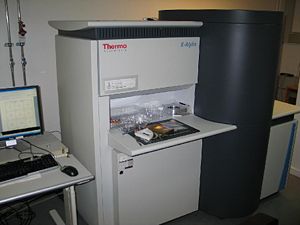
A X-ray Photoecectron Spectroscopy (XPS) system can be used at Danchip. The system is a Thermo K-Alpha system, and is found in LabManager under the name XPS-ThermoScientific.
Elemental analysis
The XPS technique can be used to do elemental analysis. A comparision about techniques and intsrumens used for elemental analysis at Danchip can be found on the page Element analysis.
XPS technique
XPS is a surface sensitive and non destructive technique used for analysis of the elemental composition. Only the outermost atomic layers (some nanometers) are probed, but with an ion gun etch it is possibile to probe deeper laying layers.
In the XPS spectrometer system the probed samples are irradiated by photons with a specific energy, and the photoelectrons that leaves the sample are detected. The energy levels of the electrons are elemental specific, and by measuring the energy of the outgoing electrons, it is possible to detect which elements that are present in a sample.
You can read futher about the technique here: [1]
The technique can be used for different purposes:
Elemental composition

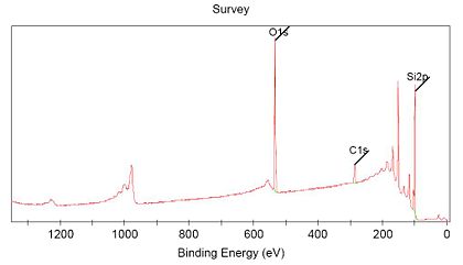
Each element give a specific "finger-print" in the XPS spectrum. The electrons in the atoms have different binding energies for all elements, and when measuring a photoelectron spectrum over a wide range of energies, the main line from each element will be placed at a specific energy in the spectra.
Here is shown a spectra measured over the energy range 0-1350 eV, and characteristic lines from three elements (C,O and Si) are seen and indicated in the spectrum.
The instrument program can use this information to give an estimate of the sample composition, giving the atomic procentage of the different elements.
Chemical state

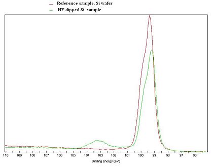
Due to the so called Chemical shift, it is possible to get information about the chemical state of the probed atoms. The core electrons of the atoms are affected, meaning that the binding energy of the electrons are slightly shifted, when an atom is bonded to atoms of other elements.
This gives an excelent tool for examining the chemistry of a surfaces, and how it is affected by different surface treatments.
If you study polymers, you can detect the precense of different chemical groups, for example (C-C),(C-OH),(C=O),(CF3) or (CF2-CH2) in the polymeric layer. And after surface treatments, you may examine differences in the polymeric layer.
Depth profiling

The analysis is made on a chosen spot on the sample surface (choosen with the system camera). The technique, is as written above, very surface sensitive and probes only the top nanometers of the sample.
With the ion beam gun on the system a etch of the sample can be done. The system measures the desired spectra, do a etch step and measures again. A series of etch cycles can be set up, measuring the composition of the sample at different depths (for example at different depth of a film).
Example: NiCr film
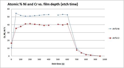
As an illustration, a figure to the left, shows an elemental analysis through a metallic film consisting of Ni and Cr. The metallic layer was about 70 nm thick, and the atomic percentage of Ni and Cr was measured through the layer.
In the graph, you see the atomic % as a function of etch depth, and it is possible to detect that the relationship between Ni and Cr is fairly constant through the metallic film.
A rough overview of XPS-ThermoScientific characteristics
| Purpose | Chemical analysis |
|
|---|---|---|
| Performance | Spot size | Can be set between 30µm - 400µm |
| Probing depth | Depending on probed element. Max probe depth lies within 10-200 Å. | |
| Resolution | Dependent on probed elements. Concentrations down to about 0,5 atomic % can in some cases be detected. | |
| Charge compensation |
Flood gun can be used for charge compensation of non conductive samples | |
| Finding structures | Choose measuring spot from camera image (magnified) | |
| Depth profiling | Purpose | With ion beam etch the top layer of the material can be removed, to do a depth profiling |
| Ion beam size | About 0,3x1 mm | |
| Substrates | Substrate size |
Max 60x60 mm |
| Substrate thickness |
Max height about 20 mm |
