Specific Process Knowledge/Characterization/XPS: Difference between revisions
| Line 20: | Line 20: | ||
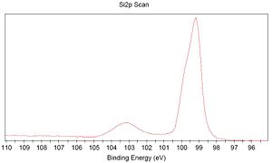
[[image:Si spectra Labadvisor.JPG|300x300px|right|thumb|XPS Si2p spectrum of Si sample]] | [[image:Si spectra Labadvisor.JPG|300x300px|right|thumb|XPS Si2p spectrum of Si sample]] | ||
==A rough overview of XPS-ThermoScientific characteristics== | ==A rough overview of XPS-ThermoScientific characteristics== | ||
Revision as of 16:34, 17 October 2011
XPS-ThermoScientific
A X-ray Photoecectron Spectroscopy (XPS) system can be used at Danchip. The system is a Thermo K-Alpha system, and is found in LabManager under the name XPS-ThermoScientific.
Elemental analysis
The XPS technique can be used to do elemental analysis. A comparision about techniques and intsrumens used for elemental analysis at Danchip can be found on the page Element analysis.
XPS technique
XPS is a surface sensitive and non destructive technique used for elemental composition analysis.
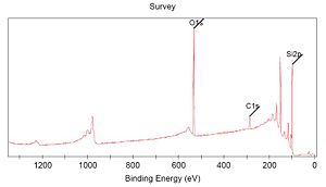
In the XPS spectrometer system the probed samples are irradiated by photons with a specific energy, and the photoelectrons that leaves the sample are detected. The energy levels of the electrons are elemental specific, and by measuring the energy of the outgoing electrons, it is possible to detect which elements that are present in a sample.


A rough overview of XPS-ThermoScientific characteristics
| Purpose | Chemical analysis |
|
|---|---|---|
| Performance | Spot size | Can be set between 30µm - 400µm |
| Probing depth | Depending on probed element. Max probe depth lies within 10-200 Å. | |
| Resolution | Dependent on probed elements. Concentrations down to about 0,5 atomic % can in some cases be detected. | |
| Charge compensation |
Flood gun can be used for charge compensation of non conductive samples | |
| Finding structures | Choose measuring spot from camera image (magnified) | |
| Depth profiling | Purpose | With ion beam etch the top layer of the material can be removed, to do a depth profiling |
| Ion beam size | About 0,3x1 mm | |
| Substrates | Substrate size |
Max 60x60 mm |
| Substrate thickness |
Max height about 20 mm |
