Specific Process Knowledge/Lithography/Aligners/Aligner: Maskless 01 processing: Difference between revisions
| Line 534: | Line 534: | ||
|} | |} | ||
The alignment test with 4 alignment marks shows a +40ppm scaling on the X-axis, as well as a 0.1mRad shearing of the axes. The result is a decent alignment in X, but a shift in Y as well as a relatively large deviation. The raw data shows the deviation in Y is due to a -40ppm scaling along the Y-axis, as seen in the MLA1-MLA1 test with 4 marks, suggesting that the scaling in Y is consistently overestimated. | The alignment test with 4 alignment marks shows a +40ppm scaling on the X-axis, as well as a 0.1mRad shearing of the axes. The result is a decent alignment in X, but a shift in Y as well as a relatively large deviation. The raw data shows the deviation in Y is due to a -40ppm scaling along the Y-axis, as seen in the MLA1-MLA1 test with 4 marks, suggesting that the scaling in Y is consistently overestimated. This is probably also why attempts to use field alignment on structures printed using a different tool always fail at the outer positions. | ||
<br>Aligning using only 2 marks yields acceptable shifts in the center of the wafer, but very large shifts in X towards the edges, as evidenced by the 7.4µm deviation in X. The raw data suggests that this deviation is mainly due to a 0.2mRad tilt in the Y-axis, which corresponds well with the 0.1mRad shearing measured using 4 marks. There is also a (-)40ppm scaling along the X-axis, again similar to what was measured during 4 mark alignment. Even a 5mm chip would be affected by the 0.2mRad tilt, so clearly 4 mark alignment is needed when aligning to a pattern that was not exposed using MLA1. | <br>Aligning using only 2 marks yields acceptable shifts in the center of the wafer, but very large shifts in X towards the edges, as evidenced by the 7.4µm deviation in X. The raw data suggests that this deviation is mainly due to a 0.2mRad tilt in the Y-axis, which corresponds well with the 0.1mRad shearing measured using 4 marks. There is also a (-)40ppm scaling along the X-axis, again similar to what was measured during 4 mark alignment. Even a 5mm chip would be affected by the 0.2mRad tilt, so clearly 4 mark alignment is needed when aligning to a pattern that was not exposed using MLA1. | ||
<br>Attempting to fix the shift in Y when using 4 alignment marks by adding 0;0 as the first mark makes no difference. And the success from the MLA1-MLA1 test when using 3 marks on the bottom half of the wafer is unfortunately not repeated for MLA3-MLA1 alignment. Using alignment marks on the top half of the wafer also doesn't change the shift. The raw data from all the alignment tests using scaling and shearing compensation (3+ marks) shows the best alignment at the bottom of the wafer, with an increasing shift in Y due to a scaling error around -40ppm. Reducing the exposed area reduces the shift in Y, but the raw data show the same trend as the large area; best alignment at the bottom of the exposed area and a scaling error in Y around -40ppm. | <br>Attempting to fix the shift in Y when using 4 alignment marks by adding 0;0 as the first mark makes no difference. And the success from the MLA1-MLA1 test when using 3 marks on the bottom half of the wafer is unfortunately not repeated for MLA3-MLA1 alignment. Using alignment marks on the top half of the wafer also doesn't change the shift. The raw data from all the alignment tests using scaling and shearing compensation (3+ marks) shows the best alignment at the bottom of the wafer, with an increasing shift in Y due to a scaling error around -40ppm. Reducing the exposed area reduces the shift in Y, but the raw data show the same trend as the large area; best alignment at the bottom of the exposed area and a scaling error in Y around -40ppm. | ||
Revision as of 12:39, 9 January 2026
Specific Process Knowledge/Lithography/authors generic
Feedback to this page: click here
Exposure technology
Aligner: Maskless 01 is not a direct laser writer. In the maskless aligner, the exposure light is passed through a spatial light modulator, much like in a video projector, and projected onto the substrate, thus exposing an area of the design at a time. The substrate is exposed by stepping the exposure field across the substrate.
The light source is a 10W 365nm LED with a FWHM of 8nm. The spacial light modulator is an 800 X 600 pixel digital micro-mirror device. The individual mirrors of the DMD are switched in order to represent the design, and are timed in order to yield the desired exposure dose, while taking into account illumination uniformity, soft-stitching, and possibly also sub-pixel features. This image is projected onto the substrate through a lens(system). The projected image yields a writing field of 400µm X 300µm, and thus a pixel size of 0.5µm X 0.5µm at wafer scale. This writing field is stepped across the substrate, in order to expose the entire design, each field overlapping slightly in order to minimize stitching errors.
The writing head of the Aligner: Maskless 01 moves only in the z-direction. Using a pneumatic focusing system, the maskless aligner is able to do real-time autofocus. The defocus process parameter is used to compensate offsets in the focusing mechanism, and to optimize printing quality in different resists and varying thicknesses. The stage of the Aligner: Maskless 01 moves only in x and y. It has no theta-axis. All rotation during alignment is thus accomplished by transformation of the input design.
Process Parameters
Exposure dose and defocus
Information on UV exposure dose
Writing speed
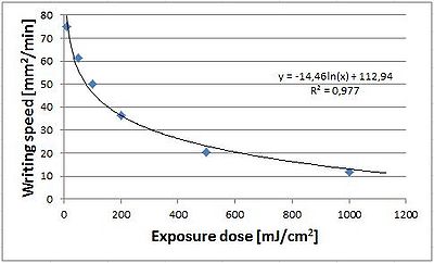
The site acceptance test performed during the installation of the Aligner: Maskless 01 showed an exposure time/speed of 0.025 min/mm2, which is slightly lower than the 0.02 min/mm2 given in the specifications. At such speeds, a full 4" design would take 2:30-3:15 hours to expose. In practice, we observe exposure times in excess of 2 hours for a full 4" design.
The exposure time increases linearly with exposure dose and writing area. However, due to the stepped nature of the exposure, the exposure time as a function of fill factor is highly nonlinear. It takes the same time to expose a single pixel as an entire 300µm X 400µm writing field, so the exposure time depends on the number of addressed writing fields, rather than on the fill factor of the design. In practice, there will probably not be much variation in exposure time with fill factor. Exposure tests using a 50mm2 design have shown that the exposure time increases linearly from 40s at 10mJ/cm2, to 257s at 1000mJ/cm2. The fill factor of the design is 39%, but ~80% of the area is addressed by the writing fields. Scaled to a full 4" wafer, the exposure time is estimated to 2:37 hours at a dose of 100mJ/cm2.
Resolution
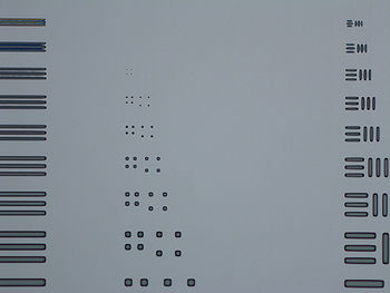
The pixel-size of the DMD in the Aligner: Maskless 01 is 0.5µm X 0.5µm (at the sample surface). The lithographic resolution of the machine is 1µm on paper, which was demonstrated in the acceptance test after installation using a resist thickness of 0.5µm. This result has later been confirmed. In 1.5µm thick resist, the resolution is around 2µm.
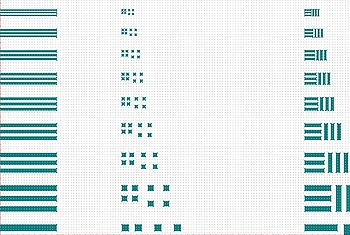
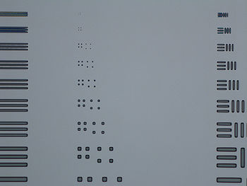
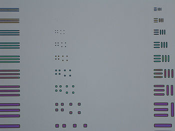
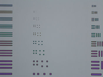
The table below shows the result of a resolution test using 1.5µm and 0.5µm positive resist. For 1.5µm resist the resolution is 2µm, maybe even a little lower, while it is 1µm, or at least close to, for 0.5µm resist. The optimal dose depends on the designed structures; dots require a lower dose in order to print to size than lines. In the case of a dark field design, trenches would probably require a lower dose in order to print to size than lines, while holes would require a higher dose to print than trenches.
Also evident in the pictures is the optical proximity effect (not to be confused with the proximity (gap) effect in contact lithography); corners are rounded, and the smallest lines show a different width for the central line compared to the outer ones. Optical Proximity Correction is the practice of augmenting the design in order achieve the desired size and shape in the finished print. A basic form of OPC is corner correction, also known as serifs, where a small square is added or subtracted at all corners. The last column in the table show the effect; the dots become square, and the short lines are the correct length. The effect of corner correction is significant below 2µm, but negligible above 4µm. The proximity effect on the width of the outer lines is not removed by corner correction; here so-called SRAFs (Sub-Resolution Assist Feature), also known as scatter bars, would be needed.
| As designed | With OPC (0.5µm corner corrections/serifs) | |
|---|---|---|
| Design file | 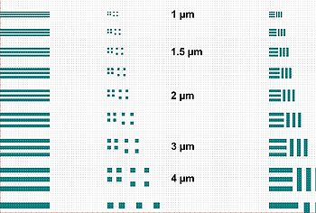
|
|
| 1.5µm AZ 5214E
Dose: 80, defoc: -3 Development: SP 60s |
|
|
| 0.5µm AZ 5214E (diluted)
Dose: 80, defoc: -3 Development: SP 30s |
|
|
Substrate positioning
During load, the machine will focus on the surface of the sample. Then, using the pneumatic focusing system, it will detect the edges of the sample (this function dependes on the substrate template used) in order to determine the center of the sample. The following results rapport findings using the "4 inch wafer" template on a standard 100mm Si substrate.
Substrate centring
During (4") substrate detection, the sample is scanned along the X- and Y-axes, as well as diagonally. From these measurements, the diameter of the substrate is calculated, as well as the stage position matching the center of the substrate. This stage position will be the default origin for the subsequent exposure.
Unfortunately, the centering does not compensate for major or minor flats. The center position will therefore typically be displaced several hundred µm from the center of the substrate along the Y-axis due to the major flat, and possibly also shifted due to any minor flats. These shifts have successfully been compensated during file conversion, which yielded a centering accuracy of ±200µm. The table below lists the corrections needed during file conversion in order to compensate for shifts due to major and minor flat, dependent on the position of the minor flat. Keep in mind that the tolerances of substrate diameter and flat lengths in the SEMI wafer standard introduce uncertainties to these numbers in the order of 0.4-0.9mm. Accurate positioning of the design relative to the substrate center would require measurement of diameter and flat lengths of the individual substrate, and subsequent recalculation of the correction values.
| Minor flat position | X correction [mm] | Y correction [mm] |
|---|---|---|
| none | 0 | -1.35 |
| left | -0.4 | -1.35 |
| up | 0 | -0.95 |
Flat alignment
At the end of (4") substrate detection, the sample is scanned twice along the flat, in order to determine the substrate rotation. This angle will be presented in the exposure panel along with the option to expose the design rotated in order to compensate for this angle, i.e. aligned to the flat.
The flat alignment accuracy has been measured to be 0±0.1° (1.7mRad) quite consistently. Out of a total of 15 exposures, 13 showed misalignment of 0.1° or better, despite initial sample rotations exceeding 5°.
Please observe, that one should not select the flat alignment option if 'Expose Crosses' is used. The design will be rotated, but the crosses will not, resulting in a subsequent alignment error equal to the flat angle.
Alignment
The alignment accuracy of the Aligner: Maskless 01 is a combination of the position accuracy of the stage, the accuracy of the alignment mark detection (mostly determined by the offset between camera and stage), and the accuracy of the pattern already on the wafer (first print).
By measuring the stitching accuracy between two layers printed on the same substrate (without unloading the substrate), we can assess the stage accuracy. By aligning to a pattern previously exposed by the Aligner: Maskless 01, we can assess the mark detection accuracy. And finally, by aligning to a pattern exposed on a different aligner, we can assess the mask-less aligner's ability to compensate for any scaling and orthogonality errors between the two machines.
Important note about correction options
You must use all available alignment corrections!
- 2 point alignment can only correct for rotation
- 3+ point alignment can correct for rotation, scaling and shearing - you must use all 3 alignment corrections!
The stage of Aligner: Maskless 01 has suffered some kind of damage (maybe during it's relocation to E-4 in 2019), which means the stage positioning is distorted. When aligning to a pattern exposed using a different machine, we typically see a shearing on the order of 0.1 mrad, i.e. the axes are not orthogonal, but even when aligning to patterns exposed on Aligner: Maskless 01 itself, this distortion results in misalignment unless a specific procedure is followed.
When aligning on Aligner: Maskless 01, you should either:
- Use only 2 alignment marks and apply rotation correction
- Use 3+ alignment marks and apply all corrections (rotation, scaling and shearing)
If 3+ marks are used, but scaling and shearing is not applied, significant misalignment will be observed, even on chips. On a 4" wafer the shift in Y can be several hundred µm.
Using only two alignment marks (on the X-axis) is recommended when aligning to patterns exposed on Aligner: Maskless 01. When aligning to patterns exposed on a different machine, using 4 alignment marks and all corrections applied yields the best alignment accuracy. The remaining error when using 4 alignment marks can be compensated by manipulating the design file. Please see the section below for details.
Alignment tests
After installation, multiple tests were conducted in order to assess the overlay accuracy of Aligner: Maskless 01. The conclusion to the early tests were that the stage accuracy is ±0.1µm, and the machine-to-self overlay accuracy is ±0.5µm. The machine-to-machine overlay accuracy was not determined (due to the lack of a suitable mask for the mask aligners). In 2019, efforts to establish regular QC of the equipment were started, and the accuracy of the alignment mark detection has been measured regularly since 2020. While both the average and the spread of the alignment errors for the x-axis (measured in 3x3 positions covering a 60x60mm2 area) has consistently been within the ±1µm specification of the machine, the spread of the alignment errors for the y-axis is typically 3±1µm, despite the average error being in spec, due to negative offsets on the upper half of the wafer and positive offsets on the lower. In 2025, it was decided to investigate this problem further, in order to determine whether a specific alignment protocol could remedy the alignment error, or whether the acceptance limits for the QC would have to be changed.
The result of these tests suggest that when aligning to a pattern exposed using MLA1, only 2 alignment marks on the X-axis should be used. If the first pattern was exposed using a different tool, 4 alignment marks must be used (with all corrections applied), but the alignment accuracy in Y-direction suffers. The Y-shift grows linearly with the size of the pattern/sample, so small samples will be less affected, while full wafers will experience shifts in Y that far exceed the ±1µm specification. In general, larger alignment error in Y must be accepted when aligning to a pattern exposed on a different tool. By scaling the design 40ppm in Y, however, it is possible to compensate for the Y-shift and achieve alignment within the machine specification across an entire wafer. Based on these results, it was decided to change the QC procedure to use only two alignment marks on the X-axis, but to keep the QC limits at ±1µm. In order to reflect the tolerance needed when using the machine, the alignment accuracy listed in the equipment performance will be changed to ±2µm.
In the MLA1-MLA1 alignment tests, the design consists of ±5µm verniers with 0.1µm resolution along the X and Y axis placed in a 3 by 3 matrix covering a 60mm by 60mm area centered on the wafer. The sample is loaded, and the first layer with linear scales is printed (without global angle). Without unloading, the second layer with vernier scales is printed on top of the first, and then the sample is developed. The deviations (±) given for the results here are calculated as half the range of measurements. If the range is small, the measurement uncertainty is used instead.
| MLA1-MLA1 | Mark positions | Rotation [mRad] | Scaling [a.u.] | Shearing [mRad] | Average error [µm] | Deviation [µm] | |
|---|---|---|---|---|---|---|---|
| No alignment
(stage accuracy test) |
X | - | - | - | - | 0.03 | ±0.05 |
| Y | - | 0.10 | ±0.225 | ||||
| Field alignment
(after development, |
X | 1: -37500; 0 2: 37500; 0 |
8.414 | - | - | 0.04 | ±0.05 |
| Y | - | -0.22 | ±0.075 | ||||
| 4 alignment marks
(like QC) |
X | 1: -37500; 0 2: 37500; 0 3: 0; 35000 4: 0; -35000 |
0.000 | 1.000001 | 0.0002 | 0.06 | ±0.05 |
| Y | 0.999960 | -0.31 | ±1.30 | ||||
| 2 alignment marks
(on X-axis) |
X | 1: -37500; 0 2: 37500; 0 |
0.003 | - | - | 0.01 | ±0.15 |
| Y | - | -0.26 | ±0.20 | ||||
| 2 alignment marks
(on Y-axis) |
X | 1: 0; 35000 2: 0; -35000 |
0.000 | - | - | 0.11 | ±0.275 |
| Y | - | -2.69 | ±0.2 | ||||
| 2 alignment marks
(top half of wafer) |
X | 1: -30000; 30000 2: 30000; 30000 |
-0.003 | - | - | 0.08 | ±0.1 |
| Y | - | -2.16 | ±0.15 | ||||
| 2 alignment marks
(bottom half of wafer) |
X | 1: -30000; -30000 2: 30000; -30000 |
0.005 | - | - | -0.26 | ±0.25 |
| Y | - | -0.01 | ±0.15 | ||||
| 2 alignment marks
(on Y-axis, starting at bottom) |
X | 1: 0; -35000 2: 0; 35000 |
0.004 | - | - | 0.02 | ±0.1 |
| Y | - | 0.02 | ±0.2 | ||||
| 5 alignment marks
(0;0 + QC marks) |
X | 1: 0; 0 2: -37500; 0 3: 37500; 0 4: 0; 35000 5: 0; -35000 |
-0.001 | 1.000003 | 0.0000 | 0.16 | ±0.05 |
| Y | 0.999963 | -1.11 | ±1.175 | ||||
| 3 alignment marks
(bottom half of wafer) |
X | 1: -30000; 0 2: 30000; 0 3: 0; -30000 |
0.006 | 1.000003 | -0.003 | -0.11 | ±0.225 |
| Y | 0.999997 | 0.13 | ±0.275 | ||||
The stage alignment test shows a relatively good repeatability of the stage. The X-axis is clearly more accurate than the Y-axis, as evidenced by the relatively large deviation on the Y-axis values. The raw data shows that all positional errors are within ±0.3µm, mainly due to the Y-shifts on the Y-axis being ~0.2µm larger than in the other positions.
The field alignment test shows much tighter values, and the errors represent the true error on the camera offset, i.e. the shift that can be corrected in the machine configuration.
The alignment test with 4 alignment marks mimics the shift from the field alignment test, but the deviation on the Y-axis is very large, probably due to the surprising -40ppm scaling measured by the alignment routine. Keep in mind that the wafer has not been unloaded between the two exposures. Something is going on with the Y-axis.
Aligning with 2 marks on the X-axis seems to fix this problem, and shows an average error similar to the camera offset, with a tight distribution across the wafer. However, aligning using 2 marks on the Y-axis introduces a large shift in Y. This shift is repeated if 2 alignment marks along the X-axis on the top half of the wafer is used, but it is fixed if 2 marks along the X-axis on the bottom half are used, or if 2 marks on the Y-axis is used with the first mark on the bottom half of the wafer. Again, there seems to be something strange going on with the Y-axis.
In an attempt to fix the large deviation on the Y-axis when using 4 alignment marks, a test was made adding an alignment mark in 0;0 as the first mark during alignment. This did not have any beneficial effect, as the deviation on the Y-axis values is similar to the deviation from the 4 mark test. Finally, inspired by the success of using two alignment marks on the bottom half of the wafer, a test using 3 alignment marks on the bottom half of the wafer was done. Strangely, this seems to fix the problem, showing no scaling of the Y-axis and yielding small shifts with reasonable deviation.
In the MLA3-MLA1 alignment tests, the design consists of ±5µm verniers with 0.25µm resolution along the X and Y axis placed in a 3 by 3 matrix covering a 60mm by 60mm area centered on the wafer. The first layer with linear scales was printed in MLA3 as QC test wafers a long time ago and subsequently patterned using lift-off of gold. These wafers are coated with resist, the second layer with vernier scales is printed in MLA1, and then the sample is developed. The deviations (±) given for the results here are calculated as half the range of measurements. If the range is small, the measurement uncertainty is used instead.
| MLA3-MLA1 | Mark positions | Rotation [mRad] | Scaling [a.u.] | Shearing [mRad] | Average error [µm] | Deviation [µm] | |
|---|---|---|---|---|---|---|---|
| 4 alignment marks
(old QC wafer) |
X | 1: -35000; -25000 2: 35000; -25000 3: -35000; 25000 4: 35000; 25000 |
7.687 | 1.000040 | -0.108 | -0,03 | ±0,625 |
| Y | 0.999979 | -1.06 | ±1,375 | ||||
| 2 alignment marks
(old QC wafer) |
X | 1: -30000; 0 2: 30000; 0 |
7.951 | - | - | -0.94 | ±7,375 |
| Y | - | -0,72 | ±0.5 | ||||
| 5 alignment marks
(old QC wafer, starting in center) |
X | 1: 0; 0 2: -35000; -25000 3: 35000; -25000 4: -35000; 25000 5: 35000; 25000 |
9.462 | 1.000040 | -0.108 | -0.22 | ±0.25 |
| Y | 0.999979 | -0.94 | ±1.5 | ||||
| 3 alignment marks
(bottom half of old QC wafer) |
X | 1: -30000; 0 2: 30000; 0 3: 0; -30000 |
19.406 | 1.000032 | -0.104 | -0.22 | ±0.5 |
| Y | 0.999981 | -1.11 | ±1.125 | ||||
| 4 alignment marks
(top half of old QC wafer) |
X | 1: -35000; 0 2: 35000; 0 3: -35000; 25000 4: 35000; 25000 |
-1.510 | 1.000041 | -0.107 | 0.17 | ±0.25 |
| Y | 0.999976 | -1.00 | ±1.375 | ||||
| 4 alignment marks
(reduced area: 30mm X 30mm) |
X | 1: -15000; -10000 2: 15000; -10000 3: -15000; 10000 4: 15000; 10000 |
-13.842 | 1.000049 | -0.113 | 0.33 | ±0.25 |
| Y | 0.999973 | -0.53 | ±0.75 | ||||
| MLA1-MLA3
(4 alignment marks) |
X | 1: -37500; 0 2: 37500; 0 3: 0; 35000 4: 0; -35000 |
-16.298 | 0.999978 | 0.106 | -0.09 | ±0.15 |
| Y | 1.000004 | 1.02 | ±0.25 | ||||
| 4 alignment marks
(second layer scaled vertically by 100.004% in CleWin) |
X | 1: -30000; -30000 2: 30000; -30000 3: -30000; 30000 4: 30000; 30000 |
-8.415 | 1.000038 | -0.103 | 0.06 | ±0.15 |
| Y | 0.999976 | -0.96 | ±0.15 | ||||
The alignment test with 4 alignment marks shows a +40ppm scaling on the X-axis, as well as a 0.1mRad shearing of the axes. The result is a decent alignment in X, but a shift in Y as well as a relatively large deviation. The raw data shows the deviation in Y is due to a -40ppm scaling along the Y-axis, as seen in the MLA1-MLA1 test with 4 marks, suggesting that the scaling in Y is consistently overestimated. This is probably also why attempts to use field alignment on structures printed using a different tool always fail at the outer positions.
Aligning using only 2 marks yields acceptable shifts in the center of the wafer, but very large shifts in X towards the edges, as evidenced by the 7.4µm deviation in X. The raw data suggests that this deviation is mainly due to a 0.2mRad tilt in the Y-axis, which corresponds well with the 0.1mRad shearing measured using 4 marks. There is also a (-)40ppm scaling along the X-axis, again similar to what was measured during 4 mark alignment. Even a 5mm chip would be affected by the 0.2mRad tilt, so clearly 4 mark alignment is needed when aligning to a pattern that was not exposed using MLA1.
Attempting to fix the shift in Y when using 4 alignment marks by adding 0;0 as the first mark makes no difference. And the success from the MLA1-MLA1 test when using 3 marks on the bottom half of the wafer is unfortunately not repeated for MLA3-MLA1 alignment. Using alignment marks on the top half of the wafer also doesn't change the shift. The raw data from all the alignment tests using scaling and shearing compensation (3+ marks) shows the best alignment at the bottom of the wafer, with an increasing shift in Y due to a scaling error around -40ppm. Reducing the exposed area reduces the shift in Y, but the raw data show the same trend as the large area; best alignment at the bottom of the exposed area and a scaling error in Y around -40ppm.
When MLA3 is used to align to a pattern printed using MLA1, the resulting spread of alignment errors is quite small, showing that MAL3 is better at compensating for the differences between the two machines than MLA1, and suggesting that the problem stems only from MLA1. A final test attempted to compensate for the observed -40ppm scaling error in Y by scaling the pattern printed using MLA1 by +40ppm (around 0;0) prior to printing. This reduces the deviation in Y, showing that it is possible to achieve good alignment even when the first pattern is printed using a different tool. Unfortunately, the scaling function during conversion doesn't seem to work, so the scaling has to be done in the design file itself, using an external layout editor. The -1µm shift in Y remained, but it should be possible to compensate for this shift either by shifting the pattern during conversion (keep in mind the shift scales with the size of the pattern) or by scaling the pattern from the bottom of the design, rather than the center.
Optimal use of the maskless aligner
As seen in the section on writing speed, the exposure speed of Aligner: Maskless 01 is around 0.02min/mm2, or 50mm2/min, at a dose of 100mJ/cm2, yielding exposure times in excess of 2 hours for a 4" wafer. At this exposure speed, we would quickly run into a bottleneck as more and more users expose more and more wafers, if full 4" designs are used all the time. Another concern is that the exposure dose seems to be unstable over long exposure times, as consecutive exposures using the same parameters have been observed to yield different lithographic results. The conclusion is that exposure using the maskless aligner requires a different design philosophy than when a mask aligner is used for the exposure.
Design philosophy
In order to effectively use the Aligner: Maskless 01, we need to steer away from the "as many variations of the design as possible" approach typically used in mask design when the design of a device is in it's test phase. Instead, we should print only one or a few devices at a time, and iterate the design based on the performance of that device, thus truly making use of the rapid prototyping capabilities of the maskless aligner.
Alternatively, we should split our design into two parts; one comprising of all the parts of the device that remain constant through the iterations, e.g. contacts, and the other part being the part of the device that is subject to design optimization. The first part should be printed using a mask aligner, while the other design can be printed much faster on the maskless aligner due to the significantly reduced exposure area. This method is especially useful if the two exposures can be done in the same layer of resist using mix-and-match resist/process.
Mix-and-match
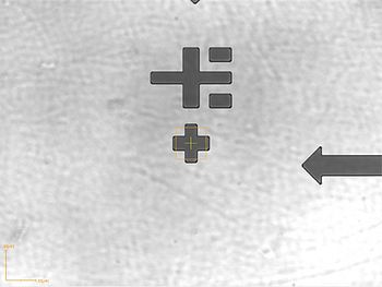
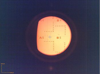
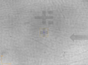
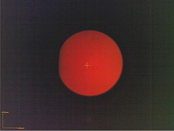
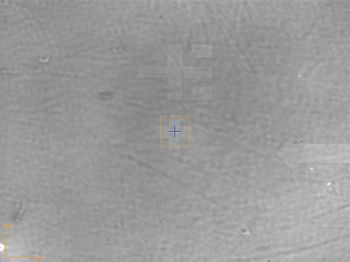
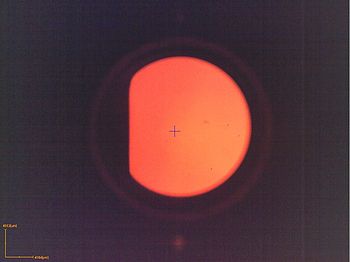
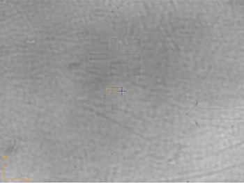
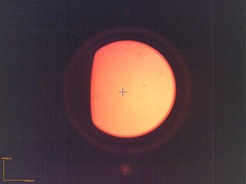
In order to establish a mix-and-match process for Aligner: Maskless 01, different resists have been tested by exposing them in a mask aligner, and subsequently aligning and exposing using Aligner: Maskless 01. Screen dumps taken during the alignment procedure may be seen in the table below. All these tests were carried out on 4" Si wafers.
The easiest approach to mix-and-match is to use a (simple) positive tone resist, such as AZ 5214E, and develop the pattern after the first exposure. The remaining resist can be exposed using the same parameters as normal, and there is plenty of contrast for the alignment process. This process can also be used if the maskless aligner is used first.
Alternatively, the post-exposure bake and/or development after first exposure can be skipped. This enables the use of AZ MiR 701, without the drop in sensitivity usually associated with a post-exposure bake at a higher temperature than the soft bake. The contrast of the alignment mark, however, is greatly reduced, making alignment more difficult. AZ MiR 701 shows more contrast than AZ 5214E, but in both cases the focus and brightness has to be optimized in order to make automatic alignment possible. The design may also have to be adapted, as the poor contrast makes navigation using the overview camera difficult. Also, a less reflective substrate than Si, e.g. oxidized Si, may complicate alignment further.
In the case of negative tone resist, such as AZ nLOF 2020, there is no contrast after exposure, making alignment impossible. Performing post-exposure bake before the second exposure yields a slight contrast, but in the case of nLOF the automatic alignment failed. Manual alignment was possible, but the alignment accuracy may suffer. For nLOF, the post-exposure bake temperature is the same as the soft bake, and post-exposure baking several times should not be a problem.
| High resolution camera | Overview camera | |
|---|---|---|
| AZ 5214E
Exposed + developed |
|
|
| AZ MiR 701
Exposed only |
|
|
| AZ 5214E
Exposed only |
|
|
| AZ nLOF 2020
Exposed + PEB |
|
|
