Specific Process Knowledge/Etch/DRIE-Pegasus/Pegasus-4/SiO2 Etch/Cr mask: Difference between revisions
| Line 263: | Line 263: | ||
</gallery> | </gallery> | ||
<gallery caption=" C10752: SiO2 etch with Cr mask on wafer piece on Si carrier | <gallery caption=" C10752: SiO2 etch with Cr mask on wafer piece on Si carrier 45 min etch, EM:0/0 H2:0sccm, C4F8:6.5sccm He:100sccm O2:10sccm, Pressure:?mTorr; platen power 25W, coil power:300W" perrow="6" widths="200px" heights="150px"> | ||
File:C10752_09.jpg | File:C10752_09.jpg | ||
File:C10752_07.jpg | File:C10752_07.jpg | ||
| Line 277: | Line 277: | ||
File:C10834T_22.jpg | File:C10834T_22.jpg | ||
</gallery> | </gallery> | ||
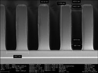
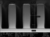
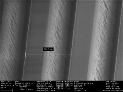
<gallery caption=" C10844: SiO2 etch with Cr mask on wafer piece on Si carrier 50 min etch, EM:0/0 H2:0sccm, C4F8:6.5sccm He:100sccm O2:10sccm, Pressure:?mTorr; platen power 20W, coil power:300W" perrow="6" widths="200px" heights="150px"> | |||
File:C10844_09.jpg | |||
File:C10844_11.jpg | |||
File:C10844_07.jpg | |||
File:C10844_05.jpg | |||
File:C10844_02.jpg | |||
File:C10844_13.jpg | |||
</gallery> | |||
===Profile, top view at tilted SEM images on 800 nm pitch and 50% duty cycle ( look at the Cr mask in top of the page=== | ===Profile, top view at tilted SEM images on 800 nm pitch and 50% duty cycle ( look at the Cr mask in top of the page=== | ||
Revision as of 11:54, 1 February 2024
Feedback to this page: click here
Unless otherwise stated, all content in this section was done by Berit Herstrøm, DTU Nanolab
SiO2 trench etching with Cr mask
| Start parameters, variations noted in the gallery headline | Recipe name: no 10 with lower platen power |
|---|---|
| Coil Power [W] | 2500 |
| Platen Power [W] | 200 |
| Platen temperature [oC] | 20 |
| H2 flow [sccm] | 25.6 |
| C4F8 flow [sccm] | 25.6 |
| He flow [sccm] | 448.7 |
| Pressure | Fully open APC valve (8-9 mTorr) |
| Electromagnetic coils (EM) 'outer coil' / 'inner coil' | '2 A' / '30 A' (PLEASE DO NOT RUN WITH THESE SETTINGS FOR MORE THAN 6 MIN) |
- 100 nm Cr mask etched in ICP metal with 500nm DUV neg resist (NUV 2300-0.5) and 65 nm barc.

Results
| Temporary conclusions on how the process parameters affect the results in this study: | What process parameters affect the results? |
|
|
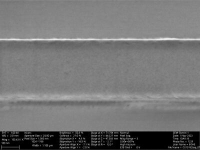
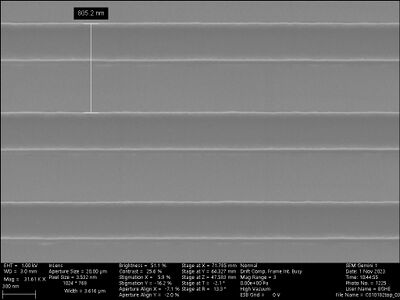
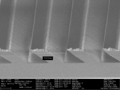
Profile SEM images
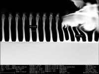
- SiO2 etch with Cr mask on full wafer 6 min etch
-
-
-

-
-
-


- SiO2 etch with Cr mask on wafer piece on Si carrier 6 min etch
-
-
-
-
-
-


- SiO2 etch with Cr mask on wafer piece on Si carrier 6 min etch, H2:0sccm
-
-
-
-
-
-


- SiO2 etch with Cr mask on wafer piece on Si carrier 6 min etch, H2:0sccm, O2:5sccm
-
-
-

-
-
-


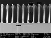
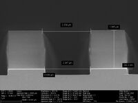
- SiO2 etch with Cr mask on wafer piece on Si carrier 6 min etch, H2:0sccm, C4F8:13sccm He:225sccm, Pressure:3.35mTorr
-
-
-
-
-
-


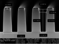
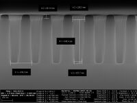
- SiO2 etch with Cr mask on wafer piece on Si carrier 6 min etch, H2:0sccm, C4F8:13sccm He:225sccm, Pressure:3.35mTorr; platen power 150W, coil power:1200W
-
-
-

-
-
-


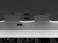
- SiO2 etch with Cr mask on wafer piece on Si carrier 6 min etch, H2:0sccm, C4F8:13sccm He:215sccm O2:10sccm, Pressure:3.6mTorr; platen power 150W, coil power:1200W
-
-
-

-
-
-


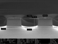
- SiO2 etch with Cr mask on wafer piece on Si carrier 6 min etch, H2:0sccm, C4F8:13sccm He:205sccm O2:20sccm, Pressure:3.6mTorr; platen power 150W, coil power:1200W
-
-
-
-
-
-
-


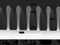
- SiO2 etch with Cr mask on wafer piece on Si carrier 6 min etch, H2:0sccm, C4F8:13sccm He:215sccm O2:10sccm, Pressure:3.6mTorr; platen power 150W, coil power:1800W
-
-
-

-
-
-


- SiO2 etch with Cr mask on wafer piece on Si carrier 6 min etch, H2:0sccm, C4F8:13sccm He:205sccm O2:20sccm, Pressure:3.6mTorr; platen power 150W, coil power:1800W
-
-
-
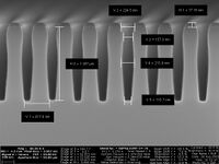
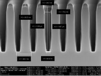
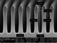
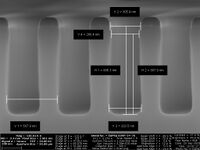
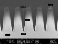
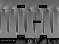
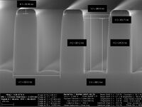
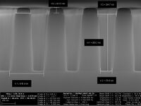
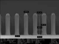
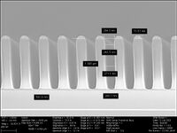
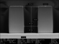
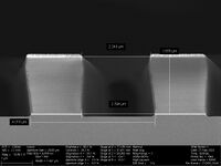
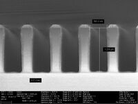
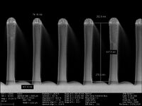
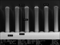
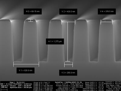
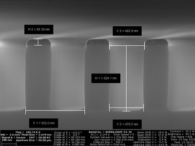
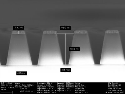
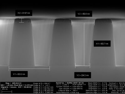
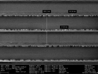
 pitch 800 nm
Top 461 nm
@edge 437 nm
bottom 402 nm
height 916 nm
height from edge 827 nm
Cr left 83.5 nm
selectivity 55.5 -
 156 nm/min
 -


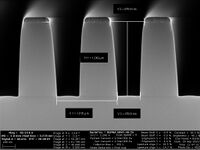
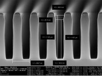
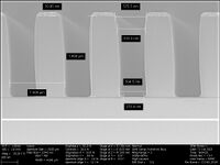
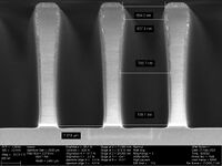
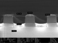
- SiO2 etch with Cr mask on wafer piece on Si carrier 6 min etch, H2:0sccm, C4F8:13sccm He:205sccm O2:20sccm, Pressure:3.6mTorr; platen power 100W, coil power:1200W
-
-
-
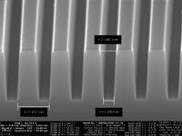
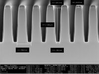
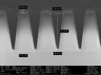
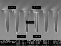
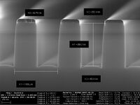
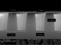
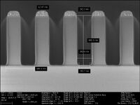
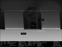
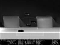
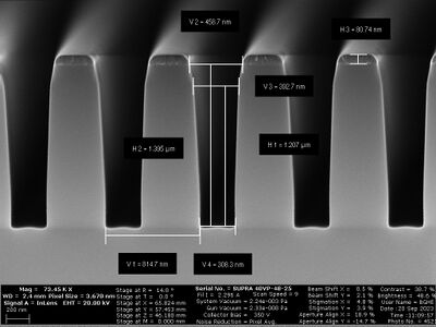
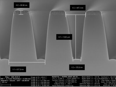
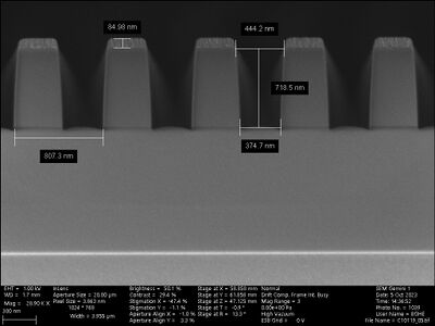
 pitch 800 nm
Top 444 nm
bottom 374 nm
height 718 nm
Cr left 85 nm
selectivity 48 -
-
-


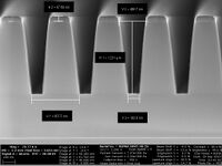
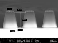
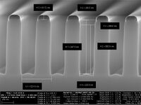
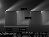
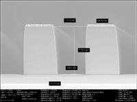
- SiO2 etch with Cr mask on wafer piece on Si carrier 14 min etch (PLEASE DO NOT REPEAT THIS LONG TIME), H2:0sccm, C4F8:13sccm He:205sccm O2:20sccm, Pressure:3.6mTorr; platen power 100W, coil power:1200W
-
-
-
-
-
-
-
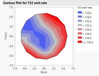 Etch on none patterned wafer, Uniformity: +- 6.4%


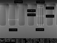
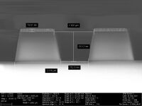
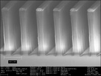
- SiO2 etch with Cr mask on wafer piece on Si carrier 10 min etch, H2:0sccm, C4F8:13sccm He:205sccm O2:20sccm, Pressure:3.6mTorr; platen power 150W, coil power:1800W
-
-
-

-
-
-


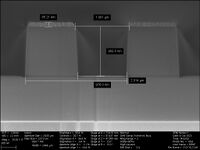
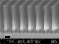
- SiO2 etch with Cr mask on wafer piece on Si carrier 14 min etch, EM:0/0 H2:0sccm, C4F8:13sccm He:205sccm O2:20sccm, Pressure:3.9mTorr; platen power 100W, coil power:1200W
-
-
-
-
-
-
-
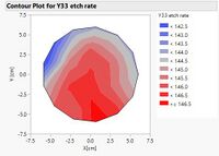 Etch on none patterned wafer, Uniformity: +-1.7%


- SiO2 etch with Cr mask on wafer piece on Si carrier 14 min etch, EM:0/0 H2:0sccm, C4F8:13sccm He:205sccm O2:20sccm, Pressure:3.9mTorr; platen power 100W, coil power:2500W
-
-
-
-
-


- SiO2 etch with Cr mask on wafer piece on Si carrier 14 min etch, EM:0/0 H2:0sccm, C4F8:13sccm He:225sccm O2:0sccm, Pressure:3.9mTorr; platen power 200W, coil power:2500W
-
-
-
-
-
-
-


- SiO2 etch with Cr mask on wafer piece on Si carrier 14 min etch, EM:0/0 H2:0sccm, C4F8:13sccm He:205sccm O2:20sccm, Pressure:3.9mTorr; platen power 200W, coil power:2500W
-
-
-
-
-
-


- SiO2 etch with Cr mask on wafer piece on Si carrier 14 min etch, EM:0/0
-
-
-
-
-
-
-
-
-


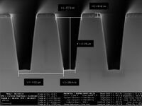
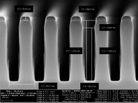
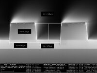
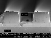
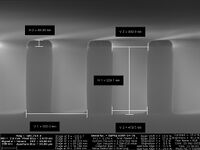
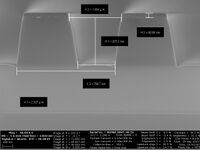
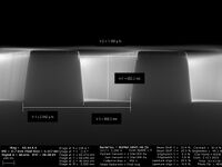
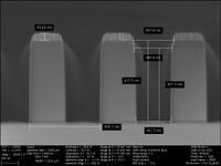
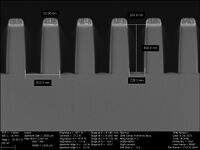
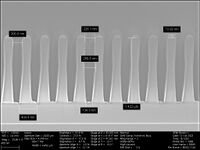
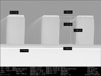
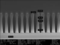
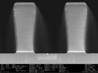
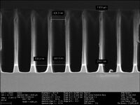
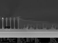
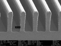
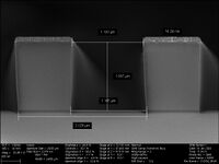
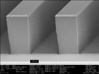
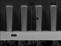
- C10751: SiO2 etch with Cr mask on wafer piece on Si carrier 20 min etch, EM:0/0 H2:0sccm, C4F8:6.5sccm He:100sccm O2:10sccm, Pressure:?mTorr; platen power 50W, coil power:600W
-
-
-
-
-
-


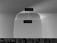
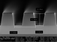
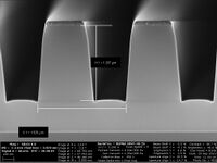
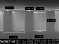
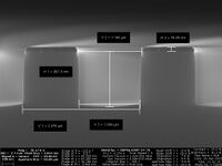
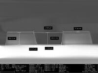
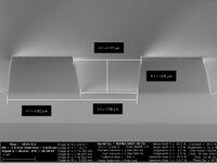
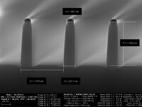
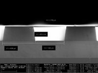
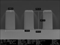
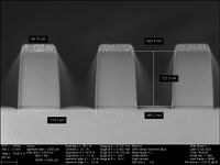
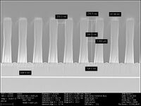
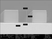
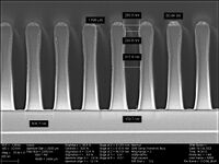
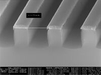
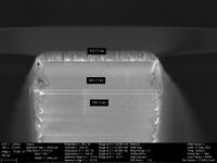
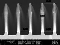
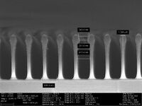
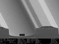
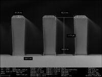
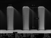
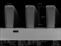
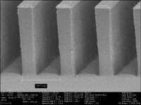
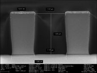
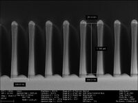
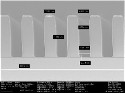
- C10752: SiO2 etch with Cr mask on wafer piece on Si carrier 45 min etch, EM:0/0 H2:0sccm, C4F8:6.5sccm He:100sccm O2:10sccm, Pressure:?mTorr; platen power 25W, coil power:300W
-
-
-
-
-
-
-
-
-
-
-
-


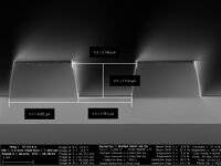
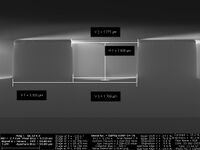
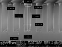
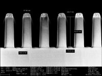
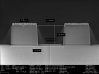
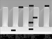
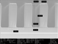
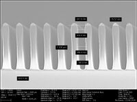
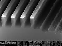
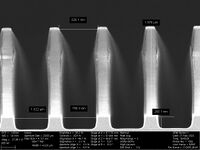
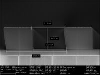
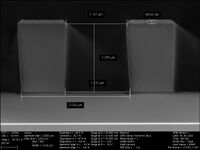
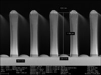
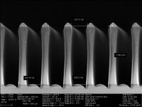
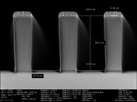
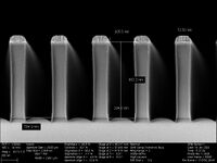
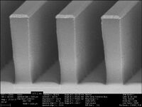
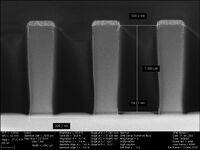
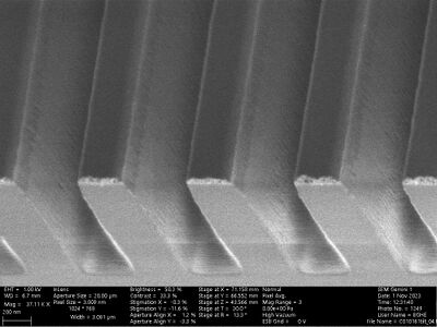
- C10844: SiO2 etch with Cr mask on wafer piece on Si carrier 50 min etch, EM:0/0 H2:0sccm, C4F8:6.5sccm He:100sccm O2:10sccm, Pressure:?mTorr; platen power 20W, coil power:300W
-
-
-
-
-
-


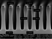
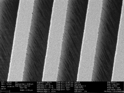
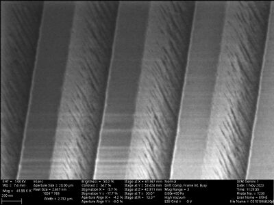
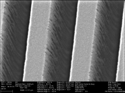
Profile, top view at tilted SEM images on 800 nm pitch and 50% duty cycle ( look at the Cr mask in top of the page
- SiO2 etch with Cr mask on full wafer 6 min etch
-
- SiO2 etch with Cr mask on wafer piece on Si carrier 6 min etch
-

- SiO2 etch with Cr mask on wafer piece on Si carrier 6 min etch, H2:0sccm
-

- SiO2 etch with Cr mask on wafer piece on Si carrier 6 min etch, H2:0sccm, O2:5sccm
-
- SiO2 etch with Cr mask on wafer piece on Si carrier 6 min etch, H2:0sccm, C4F8:13sccm He:225sccm, Pressure:3.35mTorr
-
-
-
-


- SiO2 etch with Cr mask on wafer piece on Si carrier 6 min etch, H2:0sccm, C4F8:13sccm He:225sccm, Pressure:3.35mTorr; platen power 150W, coil power:1200W
-
- SiO2 etch with Cr mask on wafer piece on Si carrier 6 min etch, H2:0sccm, C4F8:13sccm He:215sccm O2:10sccm, Pressure:3.6mTorr; platen power 150W, coil power:1200W
-
- SiO2 etch with Cr mask on wafer piece on Si carrier 6 min etch, H2:0sccm, C4F8:13sccm He:205sccm O2:20sccm, Pressure:3.6mTorr; platen power 150W, coil power:1200W
-

- SiO2 etch with Cr mask on wafer piece on Si carrier 6 min etch, H2:0sccm, C4F8:13sccm He:215sccm O2:10sccm, Pressure:3.6mTorr; platen power 150W, coil power:1800W
-
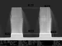
- SiO2 etch with Cr mask on wafer piece on Si carrier 6 min etch, H2:0sccm, C4F8:13sccm He:205sccm O2:20sccm, Pressure:3.6mTorr; platen power 150W, coil power:1800W
-
 pitch 800 nm
Top 461 nm
@edge 437 nm
bottom 402 nm
height 916 nm
height from edge 827 nm
Cr left 83.5 nm
selectivity 55.5
- SiO2 etch with Cr mask on wafer piece on Si carrier 6 min etch, H2:0sccm, C4F8:13sccm He:205sccm O2:20sccm, Pressure:3.6mTorr; platen power 100W, coil power:1200W
-
 pitch 800 nm
Top 444 nm
bottom 374 nm
height 718 nm
Cr left 85 nm
selectivity 48
- SiO2 etch with Cr mask on wafer piece on Si carrier 14 min etch (PLEASE DO NOT REPEAT THIS LONG TIME), H2:0sccm, C4F8:13sccm He:205sccm O2:20sccm, Pressure:3.6mTorr; platen power 100W, coil power:1200W
-

- SiO2 etch with Cr mask on wafer piece on Si carrier 10 min etch, H2:0sccm, C4F8:13sccm He:205sccm O2:20sccm, Pressure:3.6mTorr; platen power 150W, coil power:1800W
-
-
-


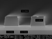
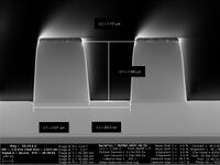
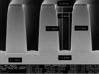
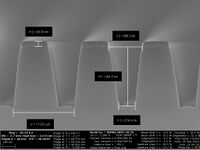
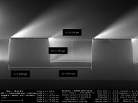
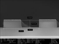
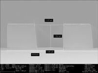
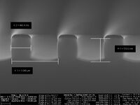
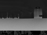
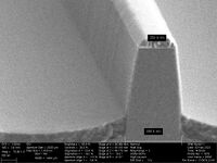
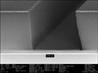
- SiO2 etch with Cr mask on wafer piece on Si carrier 14 min etch, EM:0/0 H2:0sccm, C4F8:13sccm He:205sccm O2:20sccm, Pressure:3.9mTorr; platen power 100W, coil power:1200W, the mask is removed by plasma ashing on top view and tilted view
-

-
-
-
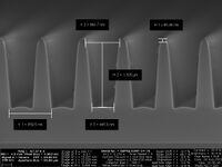
 tilt 30 degrees
 -
 tilt 30 degrees
 -
 tilt 20 degrees
 -
 tilt 20 degrees


