Specific Process Knowledge/Characterization/SEM Gemini 1: Difference between revisions
| Line 78: | Line 78: | ||
!colspan="2" border="none" style="background:silver; color:black;" align="center"|Equipment | !colspan="2" border="none" style="background:silver; color:black;" align="center"|Equipment | ||
|style="background:WhiteSmoke; color:black"|<b>SEM | |style="background:WhiteSmoke; color:black"|<b>SEM Gemini 1 (Zeiss GeminiSEM 560)</b> | ||
|- | |- | ||
!style="background:silver; color:black" align="center" valign="center" rowspan="1"|Purpose | !style="background:silver; color:black" align="center" valign="center" rowspan="1"|Purpose | ||
| Line 96: | Line 96: | ||
|style="background:LightGrey; color:black"|Resolution | |style="background:LightGrey; color:black"|Resolution | ||
|style="background:WhiteSmoke; color:black"| | |style="background:WhiteSmoke; color:black"| | ||
*1-2 nm (limited by vibrations) | *1-2 nm (limited by vibrations and acoustic noise) | ||
The resolution is strongly dependent on the type of sample and the skills of the operator | The resolution is strongly dependent on the type of sample and the skills of the operator | ||
|- | |- | ||
!style="background:silver; color:black" align="center" valign="center" rowspan="5"|Instrument specifics | !style="background:silver; color:black" align="center" valign="center" rowspan="5"|Instrument specifics | ||
Revision as of 10:51, 15 August 2023
Feedback to this page: click here
This page is written by DTU Nanolab internal

DTU Nanolab news August 2023
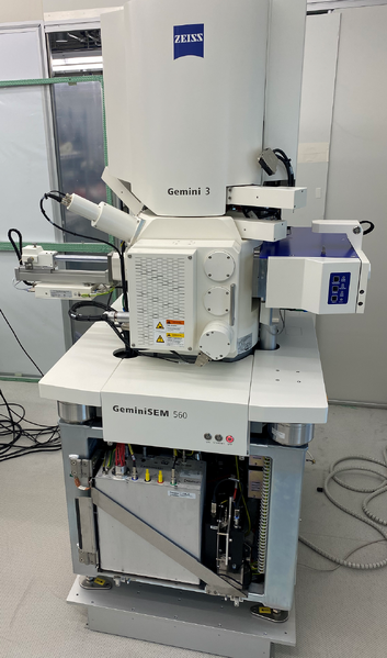
DTU Nanolab introduces next-generation SEM in the cleanroom
Right now, we are installing a new field emission scanning electron microscope (FE-SEM) in the B-section of the cleanroom. It is a state-of-the-art GeminiSEM 560 with the new Gemini 3 column from Carl Zeiss. The tool is next-generation compared to our present three about 10 years old Supra-40/60 SEM’s (also from Carl Zeiss). We are looking forward to offer our users access to all the new features provided by this tool, a.o.:
Detectors:
- SE2: Chamber mounted secondary electron (SE) detector
- In-lens SE: In-column high resolution SE detector
- In-lens EsB: In-column highly sensitive backscatter electron (BSE) detector for obtaining good material contrast
- aBSD: Retractable column mounted solid state BSE detector with six sectors for detection of energy and angle selective backscattered electrons, i.e. for obtaining both material and topographical contrast
- VPSE: Variable pressure (VP) light detector for SE signal detecting
- aSTEM: Retractable solid state STEM detector with five sectors enabling bright field and both annular and oriented dark-field transmission electron imaging
Dramatically improved performance on insulating samples achieved via two pathways:
- Latest generation column design that takes low kV imaging to the next level
- Sophisticated low vacuum modes for charge compensation:
- Standard variable pressure (VP)
- NanoVP: A retractable differential pumping aperture mounted on the column makes it possible to use the In-lens SE and ESB detectors in VP mode
Other features:
- Installed on an actively damped anti-vibration platform and with magnetic field cancellation system to protect it from external sources of noise
- Sample bias option and dedicated sample holders
- Plasma cleaner for in-situ sample and chamber cleaning
- Sample loading trough a load lock or the chamber door
- Load lock mounted camera for easy sample navigation
- Several new automated features
We will spend the coming weeks on the installation and acceptance tests of the tool and prepare the training protocol.
We hope that you will receive the tool well when we release it, which we expect to do in September.
SEM Gemini 1
The SEM Gemini 1 is a scanning electron microscope (SEM). It is a Zeiss GeminiSEM 560 .
The SEM produces enlarged images of a variety of specimens, achieving magnifications of over 500.000x providing ultra high resolution imaging. This important and widely used analytical tool provides exceptional resolution and depth of field and requires minimal specimen preparation.
The SEM is equipped with six different detectors:
- SE2: Chamber mounted secondary electron (SE) detector
- Inlens SE: In-column high resolution SE detector
- In-lens EsB: In-column highly sensitive backscatter electron (BSE) detector for obtaining good material contrast
- aBSD: Retractable column mounted solid state BSE detector with six sectors for detection of energy and angle selective backscattered electrons, i.e. for obtaining both material and topographical contrast
- VPSE: Variable pressure (VP) light detector for SE signal detecting
- aSTEM: Retractable solid state STEM detector with five sectors enabling bright field and both annular and oriented dark-field transmission electron imaging
The SEM is a VP (variable pressure) instrument, indicating that it is capable of operating at variable pressure. By increasing the pressure in the chamber it is possible to image isolating samples. The higher density of gas molecules will eliminate the charges at the cost of slightly reduced resolution. It has two different VP modes: A standard VP mode like the SEM Supra 1, 2 and 3 and a NanoVP mode. In the standard VP mode, the pressure in the chamber is increased as described above, and the dedicated VPSE detectors or the aBSED detector is used to image charging samples. In Nano VP mode, an retractable beam sleeve aperture is mounted on the column, which makes is possible to use the Inlens SE and the Inlens BSE detectors to obtains high resolution images of non-conducting samples. The SE2 and sSTEM detectors will not work in VP mode.
The SEM Gemini 1 is located in the cleanroom. It is being installed and tested in August-September 2023.
The user manual, control instruction, the user APV and contact information can be found in LabManager:
SEM Gemini 1 info page in LabManager,
Performance information
Equipment performance
| Equipment | SEM Gemini 1 (Zeiss GeminiSEM 560) | |
|---|---|---|
| Purpose | Imaging and measurement of |
|
| Location |
| |
| Performance | Resolution |
The resolution is strongly dependent on the type of sample and the skills of the operator |
| Instrument specifics | Detectors |
|
| Stage |
| |
| Electron source |
| |
| Operating pressures |
| |
| Options |
| |
| Substrates | Batch size |
|
| Allowed materials |
| |
Quality control of length measurement
| Quality Control (QC) for SEM Supra 3 | |||||||||||||||||||||||||||||||||||||||||||||||||||||||
|
QC limits:
|
