Specific Process Knowledge/Etch/ICP Metal Etcher/silicon/nano/nanoetch/180nmzep: Difference between revisions
No edit summary |
No edit summary |
||
| Line 2: | Line 2: | ||
<!--Checked for updates on 30/7-2018 - ok/jmli --> | <!--Checked for updates on 30/7-2018 - ok/jmli --> | ||
<!--Checked for updates on 5/10-2020 - ok/jmli --> | <!--Checked for updates on 5/10-2020 - ok/jmli --> | ||
{{Template:Author-jmli1}} | |||
<!--Checked for updates on 2/02-2023 - ok/jmli --> | |||
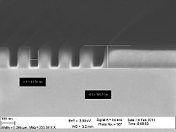
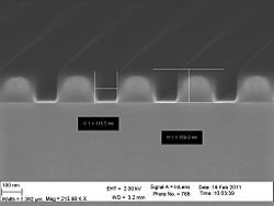
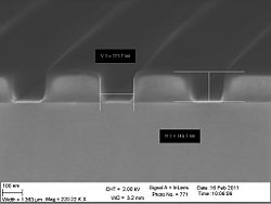
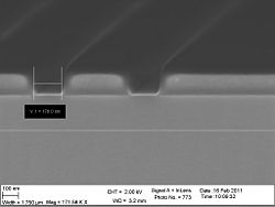
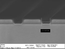
<gallery caption="The profiles of the 180 nm zep resist" widths="250" heights="200" perrow="3"> | <gallery caption="The profiles of the 180 nm zep resist" widths="250" heights="200" perrow="3"> | ||
Revision as of 16:05, 2 February 2023
Feedback to this page: click here
Unless otherwise stated, all content on this page was created by Jonas Michael-Lindhard, DTU Nanolab
- The profiles of the 180 nm zep resist
-
 The 30 nm zep profile
 -
 The 60 nm zep profile
 -
 The 90 nm zep profile
 -
 The 120 nm zep profile
 -
 The 150 nm zep profile


