Specific Process Knowledge/Lithography/EBeamLithography/JEOLPatternPreparation: Difference between revisions
| Line 58: | Line 58: | ||
Chip marks should be placed at the corners of each chip with a gap of at least 100 µm to any important structure. Bear in mind that beam scan during alignment is a high dose exposure of the mark area and hence this resist will develop (for a positive resist). This is illustrated in the microscope images below. On the left side is a global mark which has been scanned several times, both in rough scan and fine scan mode. On the right is a chip mark that has been scanned a single time in x and y. | Chip marks should be placed at the corners of each chip with a gap of at least 100 µm to any important structure. Bear in mind that beam scan during alignment is a high dose exposure of the mark area and hence this resist will develop (for a positive resist). This is illustrated in the microscope images below. On the left side is a global mark which has been scanned several times, both in rough scan and fine scan mode. On the right is a chip mark that has been scanned a single time in x and y. | ||
[[File: | [[File:9500MarkScan.png|1000px|center|frameless]] | ||
Revision as of 12:25, 31 January 2023
Feedback to this page: click here
Content and illustration by Thomas Pedersen @ DTU Nanolab unless otherwise noted.
Pattern preparation for exposure on JEOL 9500
Prior to exposure a pattern must be prepared for exposure. The original pattern must be provided in GDS format. Depending on requirements and complexity level pattern preparation will involve all or subset of the following steps.
- Placement preparation
- Alignment preparation
- Bulk and sleeve separation
- Proximity Effect Correction
- Pattern fracturing
- Field sorting
- Export for writing
Placement preparation
Pattern placement is a bit different compared to UV mask design convention and different to how our Heidelberg MLA systems work. Pattern placement is very dependent on the boundary box of the design. All patterns are placed using the ARRAY command and they are placed with respect to the center of the design boundary box. This is illustrated with the two designs, L1 and L2, below. L1 is a design nicely centered around (0,0) with a symmetric bounding box. If placed by the ARRAY command with no offset this will come out entirely as expected. L2 is however offset from (0,0) and if exported with its local bounding box and placed by the ARRAY command with no offset, it will be exposed at the center of the substrate. Thus, it is vital to keep the bounding box in mind as the ARRAY command places patterns with respect to the center of the bounding box. To get the desired result in this example, one can define an appropriate offset in the ARRAY command for exposure of L2.

Alignment preparation
Boundary box alignment
In continuation of the example above, if two layers/exposures are to be aligned to each other it is vital that the two layers boundary boxes are identical or at least symmetric around (0,0). With reference to the example below, the boundary boxes can be made identical by either
- Letting L2 inherit the L1 boundary box (option in Beamer)
- Placing small corner marks on L2 to force the boundary box as needed
Corner marks can be 1x1 nm boxes placed outside the substrate to avoid having them exposed onto the substrate.

Detection of alignment mark
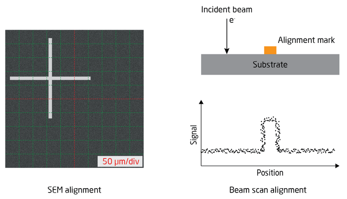
If alignment is needed it is vital to consider this already at the process design and mask design level to ensure that a visible mark is produced. Alignment is done using the electron beam in either SEM mode or beam scan mode. In SEM mode the stage is moved to the expected alignment mark position and the user will manually observe the SEM image and adjust stage position to center the mark at as high magnification as required by alignment tolerance of the design. In beam scan mode the user sets up a routine that will scan the beam across the expected mark position and the Backscatter Electron Detector (BED) will detect the backscattered signal. This is done in both x- and y-directions and system will calculate the mark center based on this.

The advantage of SEM mode is that it is fairly straight forward to do. It is however also very slow as it requires constant user input to move the stage at higher and higher magnification levels until position is sufficiently determined. Due to the time it takes it is hardly realistic to do chip alignment, only global wafer alignment should be done in this way.
Automatic alignment by beam scan is significantly faster, it only takes a couple of seconds per scan. Hence this is the only realistic way of doing chip alignment. It can however be challenging to get sufficient signal on the BED for this to work if this has not already been thought into the mask and process design. Bear in mind that the electron beam is 100 kV and unless there is a relatively high difference in atomic mass between mark and substrate the signal or contrast between substrate and mark will be too low. Gold marks on Si substrates will usually work great. Deep and narrow features etched into a substrate will also work fine. Please consult with the E-beam staff or experienced colleagues when making your mark design.
Design of global marks and chip marks
As a minimum two global alignment marks must be present on the substrate for alignment. In JEOL terms these are P and Q marks. These can be used to align a full substrate design or as initial alignment of chip arrays with individual chip marks. For chip alignment either one mark (M1) or four marks (M1-M4) must be used.

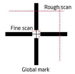
Global alignment (SETWFR) has a rough scan and a fine scan setting. Initially the mark is found using the rough scan setting, which is set to scan a long distance, typically 500 µm. Once the mark is located the machine will continue with the fine scan setting which will tyipcally scan <6 µm. In order for the machine to detect the mark on the rough scan setting the cross must have sufficient width and hence the cross is typically divided into a wide part and a slim part in the center. It is recommendable to use global marks of up to 1000 µm in height and width to make them easy and fast to find.
Chip marks are only scanned after a global alignment and hence the chip mark positions are usually very well known and the chip marks can be much smaller as indicated above.
Do NOT place any sort of text or other structures inside alignment crosses. If any other feature appear in a beam scan the system will not be able to determine which feature is the actual alignment cross.

Placement of alignment marks
Global alignment marks should be placed at the left-most and right-most part of the layout. They should however not be placed closer than 15 mm to the edge of a round wafer slot as this can interfere with height sensing of the alignment mark. If alignment marks are placed too close to the edge of a wafer slot height sensing of the marks must be disabled using the HSWITCH command.
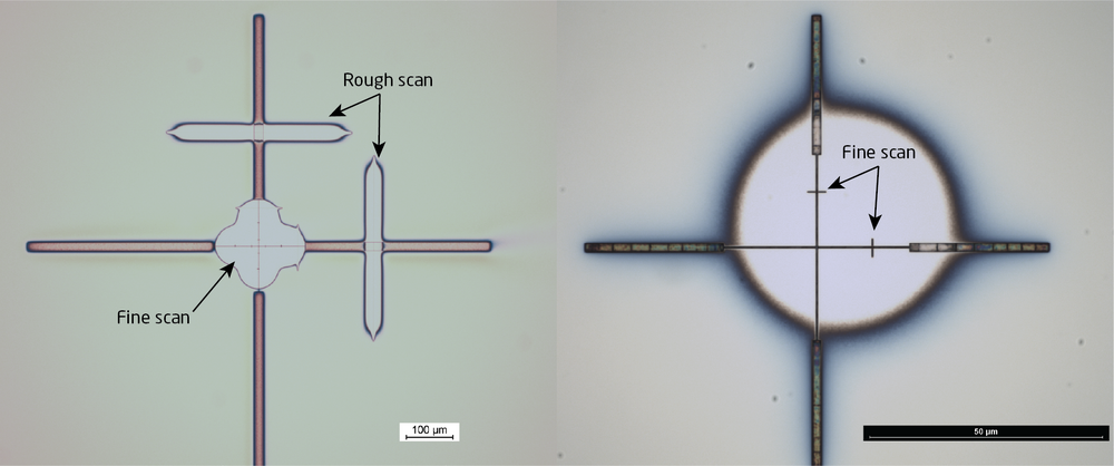
Chip marks should be placed at the corners of each chip with a gap of at least 100 µm to any important structure. Bear in mind that beam scan during alignment is a high dose exposure of the mark area and hence this resist will develop (for a positive resist). This is illustrated in the microscope images below. On the left side is a global mark which has been scanned several times, both in rough scan and fine scan mode. On the right is a chip mark that has been scanned a single time in x and y.

