Specific Process Knowledge/Lithography/nLOF: Difference between revisions
No edit summary |
No edit summary |
||
| Line 1: | Line 1: | ||
__TOC__ | |||
==Resist description== | |||
AZ nLOF 2020 is a negative UV photoresist, suitable for lift-off processes. | AZ nLOF 2020 is a negative UV photoresist, suitable for lift-off processes. | ||
==Spin coating== | ==Spin coating== | ||
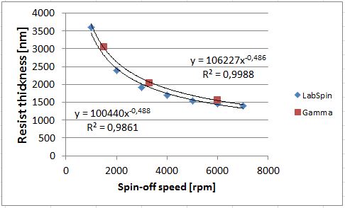
[[Image:nLOFspincurves.JPG|500x500px|thumb|Spin curves for AZ nLOF 2020 using a 30s spin-off, and a 60s@110°C softbake]] | |||
'''Typical spin parameters:''' | |||
*Spin off: 30-60 s | |||
*Soft bake: 60s @ 110°C | |||
<br clear="all" /> | <br clear="all" /> | ||
==Post-exposure bake== | ==Post-exposure bake== | ||
'''Typical PEB parameters:''' | |||
*PEB temperature: 110°C | |||
*PEB time: 60 s | |||
The recommended PEB for nLOF is 60s at 110°C, regardless of resist film thickness. | The recommended PEB for nLOF is 60s at 110°C, regardless of resist film thickness. | ||
While | '''PEB baking time investigation:''' | ||
While 60 s @ 110°C is adequate for Si substrates, less thermally conductive substrates (glass, III-V materials, chips bonded to carrier), have shown problems using the standard PEB recipe.<br> | |||
These problems were largely solved by increasing the PEB time to 120 s. Tests (on Aligner: Maskless 02) have shown that the lithographic performance of nLOF on Si is improved when using 120 s @ 110°C PEB (less stitching, less bias, more negative profile). A small report on the tests can be found [[media:nLOF_PEBtime_2019.pdf|'''here''']]. | |||
==Development== | ==Development== | ||
'''Development speed:''' | |||
*Puddle development in 2.38% TMAH (AZ 726 MIF): ~4 µm/min | |||
A | A 2 µm nLOF resist film is fully developed in 20-30 s in 2.38% TMAH (AZ 726 MIF). However, the development can be continued to 60 s in order to get a more negative resist profile (due to increased under-cut). | ||
Revision as of 16:07, 30 January 2023
Resist description
AZ nLOF 2020 is a negative UV photoresist, suitable for lift-off processes.
Spin coating

Typical spin parameters:
- Spin off: 30-60 s
- Soft bake: 60s @ 110°C
Post-exposure bake
Typical PEB parameters:
- PEB temperature: 110°C
- PEB time: 60 s
The recommended PEB for nLOF is 60s at 110°C, regardless of resist film thickness.
PEB baking time investigation:
While 60 s @ 110°C is adequate for Si substrates, less thermally conductive substrates (glass, III-V materials, chips bonded to carrier), have shown problems using the standard PEB recipe.
These problems were largely solved by increasing the PEB time to 120 s. Tests (on Aligner: Maskless 02) have shown that the lithographic performance of nLOF on Si is improved when using 120 s @ 110°C PEB (less stitching, less bias, more negative profile). A small report on the tests can be found here.
Development
Development speed:
- Puddle development in 2.38% TMAH (AZ 726 MIF): ~4 µm/min
A 2 µm nLOF resist film is fully developed in 20-30 s in 2.38% TMAH (AZ 726 MIF). However, the development can be continued to 60 s in order to get a more negative resist profile (due to increased under-cut).
