Specific Process Knowledge/Etch/ICP Metal Etcher/Chromium: Difference between revisions
Appearance
No edit summary |
No edit summary |
||
| Line 2: | Line 2: | ||
==Chromium etch in ICP metal - small substrate using carrier== | |||
The Chromium etch was carried out on the following substrate stack: | The Chromium etch was carried out on the following substrate stack: | ||
2" Si wafer with Cr laying in a 6" Si wafer with a 4" recess. The area outside the recess was covered by AZ resist. | 2" Si wafer with Cr laying in a 6" Si wafer with a 4" recess. The area outside the recess was covered by AZ resist. | ||
| Line 57: | Line 57: | ||
<br> | <br> | ||
===Chromium etch in ICP metal on a thick glass substrate | ==Chromium etch of hardmask for silicon nitride etching by Anders Simonson@nbi.ku== | ||
''Added by bghe@Nanolab'' | |||
==Chromium etch in ICP metal on a thick glass substrate== | |||
The Chromium etch has ONLY been carried out on the following substrate stack: | The Chromium etch has ONLY been carried out on the following substrate stack: | ||
The Chromium is sputter deposited onto a 2" quartz wafer and patterned by e-beam with Zep520A resist. | The Chromium is sputter deposited onto a 2" quartz wafer and patterned by e-beam with Zep520A resist. | ||
Revision as of 09:49, 27 September 2022
Feedback to this page: click here
Chromium etch in ICP metal - small substrate using carrier
The Chromium etch was carried out on the following substrate stack: 2" Si wafer with Cr laying in a 6" Si wafer with a 4" recess. The area outside the recess was covered by AZ resist. The work was carried out be Erol Zekovic @Nanotech and BGHE@nanolab
| Parameter | Cr etch |
|---|---|
| Cl2 (sccm) | 65 |
| O2 (sccm) | 15 |
| Pressure (mTorr) | 15 |
| Coil power (W) | 300 |
| Platen power (W) | 15 |
| Temperature (oC) | 50 |
| Spacers (mm) | 100 |
| Etch rate (nm/min) | ~32 (Date: 2014-08-13) |
| Zep520A resist selectivity | NA |
| Comment | Was masked by capton tape |
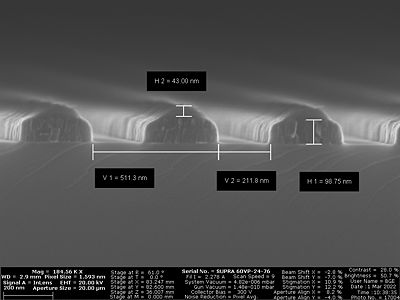
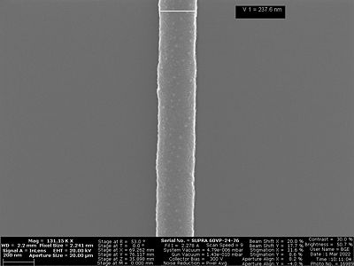
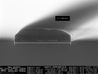
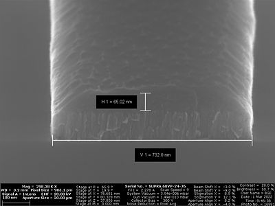
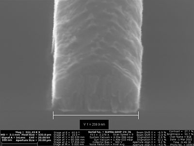
- Etching lines in 100nm Cr with the Cr etch for 3 min with 300 nm DUV resist BGHE@Nanolab Feb 2022
Chromium etch of hardmask for silicon nitride etching by Anders Simonson@nbi.ku
Added by bghe@Nanolab
Chromium etch in ICP metal on a thick glass substrate
The Chromium etch has ONLY been carried out on the following substrate stack: The Chromium is sputter deposited onto a 2" quartz wafer and patterned by e-beam with Zep520A resist. This 2" QZ wafer is bonded with crystal bond to a 65mmx65mm quartz plate with the thickness: 6.35mm. This QZ plate is bonded to a Si wafer.
| Parameter | Cr etch |
|---|---|
| Cl2 (sccm) | 65 |
| O2 (sccm) | 15 |
| Pressure (mTorr) | 15 |
| Coil power (W) | 300 |
| Platen power (W) | 15 |
| Temperature (oC) | 50 (no back side cooling) |
| Spacers (mm) | 100 |
| Etch rate (nm/min) | ~14 |
| Zep520A resist selectivity | ~0.9 |
| Comment | . |

