Specific Process Knowledge/Lithography/EBeamLithography/eLINE: Difference between revisions
| Line 62: | Line 62: | ||
|} | |} | ||
Beware that AR-N 8200 exposure result is extremely dependent on PEB process. Refer to AR-N 8200 page for more information. | Beware that AR-N 8200 exposure result is extremely dependent on PEB process. Refer to [[Specific_Process_Knowledge/Lithography/ARN8200|AR-N 8200]] page for more information. | ||
==Typical beam currents== | ==Typical beam currents== | ||
Revision as of 11:24, 8 August 2022
THIS PAGE IS UNDER CONSTRUCTION
Process information for the Raith eLINE Plus system
The system was installed in the cleanroom in May 2022. As we get more familiar with the tool this page will be populated with relevant process information.
Dose information

The eLINE tool operates with four different design element types; area, curved elements, line and dot. The element types are classified as:
- Area: Polygons
- Curved elements: Elements that have an adjustable radius
- Line: Zero-width line
- Dot: Single point/vertice element
The software allows the user to define different doses for the four different types of elements and thus it is essential to know how the design is drawn and interpreted. The units used are:
- Area dose [µC/cm2],
- Curved element dose [µC/cm2]
- Line dose [pC/cm]
- Dot dose [pC].
Also notice that the unit prefix changes from micro to pico. We recommend setting the same dose for area and curved elements.
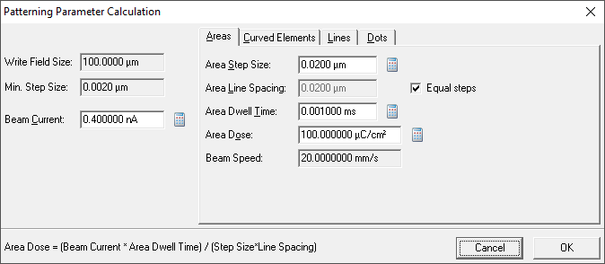
The dose for each type can be setup under the "Patterning Parameter". Before updating the requested dose the beam current must be measured from the "Patterning Parameter" page. In all tabs the user will set a step size, i.e. the distance between beam positions and a dose. The dwell time must then be updated by clicking the calculate icon next to the dwell time field. The dwell time will be calculated based on the last beam current measurement.
Dot dose, line dose and curved element doses can be disabled in the Patterning Parameter window and in that case the system will IGNORE the type of elements that are disabled, i.e. they will not be written.
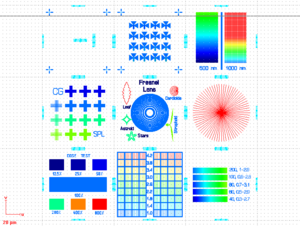
We recommend all EBL users to do a dose test prior to exposing samples of significant value. As a starting point you can consider to use the Demo.csf provided on the tool. This pattern is available in the auto generated user folder. The pattern consist of areas, curved elements, lines and dots as shown below.

Table of dose to clear (area or curved elements) on Si substrate
| Dose [µC/cm2] | |||
|---|---|---|---|
| Acc. voltage | AR-P 6200.09 (180 nm) | PMMA 950k | AR-N 8200.06 |
| 10 kV | 30 | ||
| 20 kV | 70 | ||
| 30 kV | 100 | 200 | |
Beware that AR-N 8200 exposure result is extremely dependent on PEB process. Refer to AR-N 8200 page for more information.
Typical beam currents
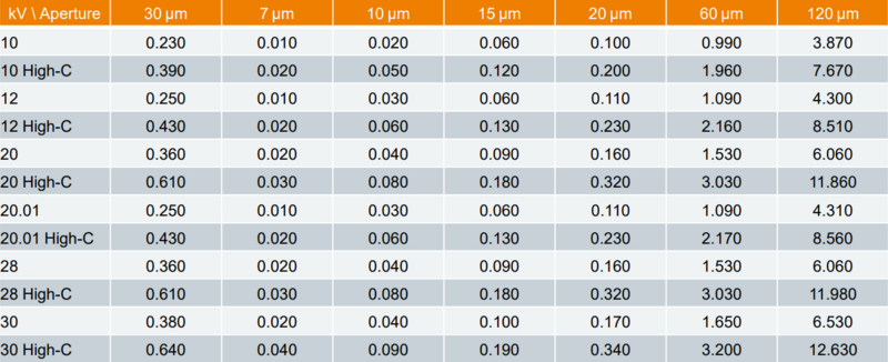
Beam current is a function of acceleration voltage and aperture and thus beam current is locked by the choice of acceleration voltage and aperture. Typical beam currents are given in the table below. Writing time can be estimated in the software once a job is defined, it is however straight forward to estimate in advance based on area to pattern, A, dose to clear, d0, and beam current, I as: T = d0*A/I

Writing fields
Aspects of WF, dimension and resolution, step size
