Specific Process Knowledge/Thin film deposition/Deposition of Silicon Oxide/Deposition of Silicon Oxide using Lesker sputter tool: Difference between revisions
| Line 85: | Line 85: | ||
The "SiO<sub>2</sub> target (RF sputter)" study was done on clean Si substrates. The sputter power was 157W and the pressure 3.5 mTorr using RF sputtering of a SiO<sub>2</sub> target. The film thicknesses were around 42 nm. | The "SiO<sub>2</sub> target (RF sputter)" study was done on clean Si substrates. The sputter power was 157W and the pressure 3.5 mTorr using RF sputtering of a SiO<sub>2</sub> target. The film thicknesses were around 42 nm. | ||
<b>From SiO<sub>2</sub> target (RF sputter)</b> | |||
{| {{table}} border="1" cellspacing="0" cellpadding="8" | {| {{table}} border="1" cellspacing="0" cellpadding="8" | ||
| align="center" style="background:#f0f0f0;"|'''Wafer nr''' | | align="center" style="background:#f0f0f0;"|'''Wafer nr''' | ||
Revision as of 17:40, 18 July 2022
Feedback to this page: click here
Sputter deposition of SiO2 using Sputter-System (Lesker)
SiO2 can be sputter deposited in the Sputter-System (Lesker). You will find information on the pressure, max power and expected deposition rate on the Equipment page here in LabAdviser. To see the deposition parameters used by others, search the Process Log in LabManager.
SiO2 Reacrive RF Sputtering from Si target
This page presents the results of reactive SiO2 deposition using RF sputtering with oxygen in Sputter-System Lesker, now commonly known as "Old Lesker". The deposition target is Si. Source #5 (RF) was used. R-RF SiO2 is commonly used for the dielectric layers, especially if lift-off is needed.
The fabrication and characterization described below were conducted in 18 of March 2022 by Evgeniy Shkondin, DTU Nanolab. The prepared samples were investigated by the Spectroscopic Ellipsometry. The Sellmeier optical model is used. The focus of the study was the deposition conditions for possible backup in case of Cluster Lesker failure.
The process recipe in a Sputter-System (Lesker) is following:
- Deposition type: R-RF
- Power: 90 W.
- Pressure: 3 mTorr
- Gas: 10% of O2 in Ar
- Deposition time: 7200 s.
- Temperature: 20°C (no heating)
- Measured DC bias: 400V
Measured thickness: 170nm for 7200s (Measured by Spectroscopic Ellipsometry. The substrate used: 100mm Si wafer)
- Deposition Rate: 0.023 nm/s
- Uniformity measurements and optical function.
-
 Uniformity across 100 wafer.
 -
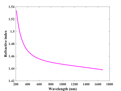 Measured refractive index.


| Deposition results on 150mm wafers | ||||
|---|---|---|---|---|
| Time (s) | Average thickness (nm) | Standard deviation error | Minimum thickness (nm) | Maximum thickness (nm) |
| 7200 | 168.85 | 4.55 | 163.21 | 177.23
|
Two important notes:
- 1. Keep the pressure around 3 mTorr. If pressure increases to 5mTorr the deposition rate will suffer so practically the sputtering stops.
- 2. Do not increase oxygen levels above 10% for the same reason as above.
Non reactive SiO2 deposition from SiO2 target
SiO2 can also be sputtered directly from SiO2 target with RF bias assistance in the Sputter-System (Lesker).
Below you will find the deposition parameters and results of a study on the surface roughness and oxide insulation quality of the sputtered SiO2.
Surface roughness optimization
By Bjarke Thomas Dalslet @Nanotech.dtu.dk
The Lesker CMS 18 sputter system provides thin films of varying surface roughness. This roughness was verified to be dependent on the sputtered material, sputter mode (DC or RF) and the substrate bias strength. Other probable factors include sputter power and pressure. Below is a table of results for SiO2. Similar studies were carried out for Si and Ta.
The "SiO2 target (RF sputter)" study was done on clean Si substrates. The sputter power was 157W and the pressure 3.5 mTorr using RF sputtering of a SiO2 target. The film thicknesses were around 42 nm.
From SiO2 target (RF sputter)
| Wafer nr | RF bias (W) | Reactive O2 (%) | Power(W) | Rq (RMS) (nm) | Thickness (nm) |
| 3 | 0 | 0 | 157 | 0.902 | |
| 6 | 5 | 0 | 157 | 0.499 | 44 |
| 7 | 10 | 0 | 157 | 0.142 | 42 |
| 8 | 15 | 0 | 157 | 0.422 | 40 |
Oxide insulation analysis
by Bjarke Thomas Dalslet @Nanotech.dtu.dk
The wafers in this analysis consisted of a Si substrate with no native oxide. A layer of SiO2 was reactively sputtered (9% O2 90 W 3.5 mTorr). After that, using a shadow mask, 200nm thick gold rectangles was electro deposited on top of the oxide. Gold was also electro deposited on the back side. Then the impedance as a function of frequency was recorded.
The figure shows the measurements for different oxide thicknesses. Most of the measurements show perfect capacitors, although for illustration measurements with a few pinholes and with many pinholes is also shown for the 20 nm sample.
The success rate for the different thicknesses can be seen in the table, together with the number of samples measured and the number of perfect capacitors.
It is possible to make perfect capacitors with oxide thicknesses down to and including 5 nm and possibly even thinner, although the failure rate increases. Bear in mind, though that each structure measured here has an area of 8 mm2 - for a 1 mm2 structure the failure rate would be much lower, assuming the short circuits are not located on the sides of the structures.

| Name | Thickness [nm] | # samples measured | # good capacitors | Success rate [%] |
| 38 | 5 | 11 | 1 | 9 |
| 39 | 10 | 10 | 2 | 20 |
| 40 | 20 | 7 | 3 | 43 |
| 41 | 30 | 7 | 7 | 100 |
| 37 | 50 | 7 | 7 | 100 |