Specific Process Knowledge/Characterization/Profiler: Difference between revisions
| Line 103: | Line 103: | ||
==Stylus Profiler (Tencor P17) [[Image:section under construction.jpg|70px]]== | ==Stylus Profiler (Tencor P17) [[Image:section under construction.jpg|70px]]== | ||
The P17 Stylus Profiler from KLA Tencor is used in a similar manner to the Dektak XTA for profiling surfaces with structures in the micro- and | The P17 Stylus Profiler from KLA Tencor is used in a similar manner to the Dektak XTA for profiling surfaces with structures in the micro- and submicrometer range as well as stress mapping and roughness measurements. It has more advanced options for stress measurements than the Dektak XTA and allows the user to measure a stress map with down to 5° radial resolution. | ||
A line profile measurement can be done across a specific structure by using a high magnification camera to locate the structure. It is also possible to program the stylus to measure many parallel scans, mapping out a surface, or to program a sequence of scans in different locations on a wafer defined with respect to some deskew points. [[Specific_Process_Knowledge/Characterization/Stress_measurement|Stress measurements]] of thin films on a wafer can be done by measuring the wafer's curvature. | A line profile measurement can be done across a specific structure by using a high magnification camera to locate the structure. It is also possible to program the stylus to measure many parallel scans, mapping out a surface, or to program a sequence of scans in different locations on a wafer defined with respect to some deskew points. [[Specific_Process_Knowledge/Characterization/Stress_measurement|Stress measurements]] of thin films on a wafer can be done by measuring the wafer's curvature. | ||
| Line 109: | Line 109: | ||
A disadvantage of the P17 is that is can be hard to locate the structures one wants to measure as the maximum field of view of the camera is 1x1.5 mm. We recommend knowing your sample well or having a picture of the sample design available so you can easily locate the features of interest. | A disadvantage of the P17 is that is can be hard to locate the structures one wants to measure as the maximum field of view of the camera is 1x1.5 mm. We recommend knowing your sample well or having a picture of the sample design available so you can easily locate the features of interest. | ||
Otherwise the P17 is easy to use, fast and | Otherwise the P17 is easy to use, fast and very reliable in its measurement accuracy, just like the DektakXT. | ||
'''The user manual, quality control procedure and results, technical information and contact information can be found in LabManager:''' | '''The user manual, quality control procedure and results, technical information and contact information can be found in LabManager:''' | ||
| Line 121: | Line 121: | ||
===Equipment performance and process related parameters Stylus Profiler (Tencor P17)=== | ===Equipment performance and process related parameters Stylus Profiler (Tencor P17)=== | ||
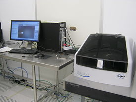
[[image:KLA-Tencor P17 profiler.JPG|275x275px|right|thumb|Front of the P17 profiler located in cleanroom F-2.]] | |||
{| border="2" cellspacing="0" cellpadding="10" | {| border="2" cellspacing="0" cellpadding="10" | ||
|- | |- | ||
!style="background:silver; color:black;" align="left"|Purpose | !style="background:silver; color:black;" align="left"|Purpose | ||
|style="background:LightGrey; color:black"|Profiler for measuring | |style="background:LightGrey; color:black"|Profiler for measuring microstructures||style="background:WhiteSmoke; color:black"| | ||
*Single line profiles | *Single line profiles | ||
*Wafer mapping | *Wafer mapping | ||
*[[Specific_Process_Knowledge/Characterization/Stress_measurement|Stress measurements]] by measuring wafer bow | *[[Specific_Process_Knowledge/Characterization/Stress_measurement|Stress measurements]] by measuring the wafer bow | ||
*Surface roughness on a line scan | *Surface roughness on a line scan | ||
|- | |- | ||
| Line 135: | Line 135: | ||
|style="background:LightGrey; color:black"|Scan range x y | |style="background:LightGrey; color:black"|Scan range x y | ||
|style="background:WhiteSmoke; color:black"| | |style="background:WhiteSmoke; color:black"| | ||
Line scan x: | Line scan x: up to 200 mm in a single scan. No stitching. | ||
Map scan xy: any rectangle that can be inscribed in a 200 mm circle but note limited resolution (max. 4 million points) | |||
- | |||
|style="background:LightGrey; color:black"|Scan range z | |style="background:LightGrey; color:black"|Scan range z | ||
|style="background:WhiteSmoke; color:black"| | |style="background:WhiteSmoke; color:black"| | ||
50 | 50 nm to 900 µm (it is possible to measure smaller steps but not recommended as the results may not be accurate) | ||
|- | |- | ||
|style="background:LightGrey; color:black"|Resolution x y | |style="background:LightGrey; color:black"|Resolution x y | ||
|style="background:WhiteSmoke; color:black"| | |style="background:WhiteSmoke; color:black"| | ||
Down to 0. | Down to 0.025 µm | ||
|- | |- | ||
|style="background:LightGrey; color:black"|Resolution z | |style="background:LightGrey; color:black"|Resolution z | ||
|style="background:WhiteSmoke; color:black"| | |style="background:WhiteSmoke; color:black"| | ||
0.01 Å, 0.08 Å, or 0.6 Å according to the manufacturer for ranges 13 µm, 131 µm, and 1 mm.* | |||
|- | |- | ||
|style="background:LightGrey; color:black"|Height accuracy z (95 % confidence) | |style="background:LightGrey; color:black"|Height accuracy z (95 % confidence) | ||
| Line 173: | Line 174: | ||
|- | |- | ||
|} | |} | ||
*The resolution for the smallest range is theoretical, as this is below the noise threshold at least in our lab. | |||
===Height measurement accuracy for the Tencor P17 Stylus Profiler === | ===Height measurement accuracy for the Tencor P17 Stylus Profiler === | ||
Revision as of 13:23, 24 November 2021
Feedback to this page: click here
Overview of the Nanolab profilers
All the profilers are compared on the topographic measurement page.
The sections below describe each profiler (stylus profilers and optical profilers) in more detail.
Dektak XTA stylus profiler
The Dektak XTA stylus profiler from Brüker is used for profiling surfaces of samples with structures in the micro- and nanometer range. The size of the structures that can be measured is limited by the tip dimensions.
A profile measurement can be done across a specific structure by using a high magnification camera to locate the structure. It is also possible to program the stylus to measure in several positions, defined with respect to some deskew points. Stress measurements of thin films can be done by measuring the wafer bow.
The user manual, quality control procedure and results, technical information and contact information can be found in LabManager:
| Purpose | Profiler for measuring micro structures |
|
|---|---|---|
| Performance | Scan range x y |
Line scan x: 50 µm to 55 mm in a single scan, up to 200 mm with stiching |
| Scan range z |
50 Å to 1 mm | |
| Resolution x y |
Down to 0.003 µm | |
| Resolution z |
1 Å, 10 Å, 80 Å or 160 Å (for ranges 65 kÅ, 655 kÅ, 5240 kÅ and 1 mm respectively) | |
| Height accuracy z (95 % confidence) |
~ 300 Å for the 65 kÅ range, ~ 0.17 µm for the intermediate ranges, and ~0.6 µm for the 1 mm range for well-defined steps that are easy to measure reproducibly (see below) | |
| Max scan depth as a function of trench width W |
1.2*(W[µm]-5µm) | |
| Hardware settings | Tip radius |
|
| Substrates | Substrate size |
|
| Substrate materials allowed |
|
Height measurement accuracy for the DektakXT
The accuracy of a height measurement with the profiler depends on the measurement settings, the sample, the instrument calibration and the resolution.
Use the right measurement settings for your sample
Both the force setting and the scan speed are important: Too high force may compress a soft material like Al, Au or some polymers, while too low force may lead to the stylus "jumping" over features, especially if the scan speed is high.
If the scan speed is too low and you are measuring a small step <500 nm, you may experience drift in the measurement. Of course you also must make sure the feature you are measuring is wide enough for the stylus tip to reach the bottom (see the DektakXT manual, Figure 3 for details).
A sharp vertical step is easiest to measure. If the step is gradual or the surface is very rough, it can be difficult to determine where to measure and how the scan should be leveled.
Influence of calibration standard uncertainty
Nanolab staff check the instrument's measurement accuracy with a standard step height of 9160 Å for the 65 kÅ range and 24.865 µm for the larger ranges. The 95 % confidence intervals for the standards are 300 Å for the 9160 Å standard and 0.15 µm for the 24.865 µm standard. If the control measurement is beyond the limit set in our Quality Control procedure, the instrument is calibrated and the users informed (see LabManager for details on the control instruction and the control measurement data).
The size of the calibration standard confidence intervals mean that the measurement uncertainty is much more significant for very shallow steps below 500-1000 nm than for steps in the micron range: The 95 % confidence interval in the 65 kÅ range is obviously at least ± 30nm, so measuring a 100-200 nm step will have a large error percentage-wise. Note that this error (from the calibration standard) is systematic. The random error associated with repeated measurements is usually smaller (perhaps ± 5 nm). One can therefore measure shallow steps to compare samples even if the absolute numbers are not very reliable.
Total uncertainty
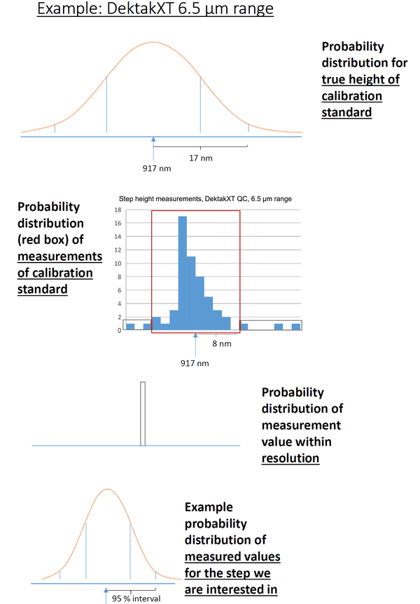
To estimate the accuracy of the Dektak's measurements we have to combine the error of the calibration with the error from the limit on the resolution and the scatter of repeated measurements. This is shown graphically on the right. You can see an uncertainty budget for the Dektak measurements here (made by Rebecca Ettlinger in 2020): Media:uncertainty budget dektaks.xlsx. It is based on the procedure described here.
The error stemming from the uncertainty on the calibration standard dominates for all ranges except the 1 mm range, where the resolution also plays a role. This leads to the 95 % confidence intervals listed above in the table: just over 30 nm for the smallest range, about 0.17 µm for the medium ranges, and about 0.6 µm for the 1 mm range. As noted above, be aware that if you have a step height that is difficult to measure, the scatter of repeated measurements could easily lead to larger confidence intervals.
Stylus Profiler (Tencor P17) 
The P17 Stylus Profiler from KLA Tencor is used in a similar manner to the Dektak XTA for profiling surfaces with structures in the micro- and submicrometer range as well as stress mapping and roughness measurements. It has more advanced options for stress measurements than the Dektak XTA and allows the user to measure a stress map with down to 5° radial resolution.
A line profile measurement can be done across a specific structure by using a high magnification camera to locate the structure. It is also possible to program the stylus to measure many parallel scans, mapping out a surface, or to program a sequence of scans in different locations on a wafer defined with respect to some deskew points. Stress measurements of thin films on a wafer can be done by measuring the wafer's curvature.
A disadvantage of the P17 is that is can be hard to locate the structures one wants to measure as the maximum field of view of the camera is 1x1.5 mm. We recommend knowing your sample well or having a picture of the sample design available so you can easily locate the features of interest.
Otherwise the P17 is easy to use, fast and very reliable in its measurement accuracy, just like the DektakXT.
The user manual, quality control procedure and results, technical information and contact information can be found in LabManager:
Info about using the analysis software from outside the cleanroom:
Apex software access
| Purpose | Profiler for measuring microstructures |
| ||
|---|---|---|---|---|
| Performance | Scan range x y |
Line scan x: up to 200 mm in a single scan. No stitching. Map scan xy: any rectangle that can be inscribed in a 200 mm circle but note limited resolution (max. 4 million points) - |
Scan range z |
50 nm to 900 µm (it is possible to measure smaller steps but not recommended as the results may not be accurate) |
| Resolution x y |
Down to 0.025 µm | |||
| Resolution z |
0.01 Å, 0.08 Å, or 0.6 Å according to the manufacturer for ranges 13 µm, 131 µm, and 1 mm.* | |||
| Height accuracy z (95 % confidence) |
~ 300 Å for the 65 kÅ range, ~ 0.17 µm for the intermediate ranges, and ~0.6 µm for the 1 mm range for well-defined steps that are easy to measure reproducibly (see below) | |||
| Max scan depth as a function of trench width W |
1.2*(W[µm]-5µm) | |||
| Hardware settings | Tip radius |
| ||
| Substrates | Substrate size |
| ||
| Substrate materials allowed |
|
- The resolution for the smallest range is theoretical, as this is below the noise threshold at least in our lab.
Height measurement accuracy for the Tencor P17 Stylus Profiler
Similar to what the text says for Dektak XTA...
-->
Optical Profiler (Sensofar S Neox)
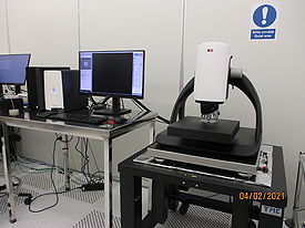
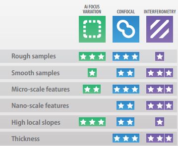
The Sensofar S Neox 3D Optical Profiler has a sensor head that combines confocal, interferometry and focus variation techniques as well as thick and thin film measurement capabilities.
The Neox sensor head provides standard microscope imaging, confocal imaging, confocal profiling, PSI (Phase Shift Interferometry), CSI (Coherence Scanning Interferometry), Active illumination (Ai) Focus Variation and high resolution thin film thickness measurements on a single instrument.
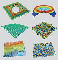
The main purpose is 3D topographic imaging of surfaces, step height measurements in smaller trenches/holes than can be obtained with standard stylus methods (i.e. with aspect ratios higher that 1:1), roughness measurements with larger FOV (Field Of View) than the AFM, but less horisontal resolution.
For most samples the optical profiler provides fast and easy information without any sample preparation. However, it can be necessary to cover thin transparent layers (< 2 µm) with a thin layer of metal.
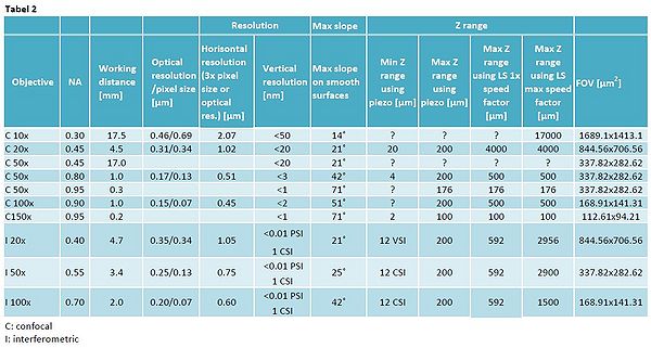
The resolution is limited by the objectives and the pixel resolution.
Analysis software:
- Free analysis software for visualizing and analyzing AFM and Optical profiler files (Sensofar) Gwyddion
- SensoView software from Sensfar want also be downloaded for all users: U:\Nlab\CleanroomDrive\_Equipment\Optical profiler Sensofar\SensoVIEW 1.6.0
The user manual, technical information (SensoSCAN and SensoVIEW manuals) and contact information can be found in LabManager:
Optical profiler (Sensofar S Neox) info page in LabManager
Process Information
- Sensofar presentation on how the sensofar works (for the previous system but the techniques are the same)
- S Neox leaflet including specifications
- Results from the Optical Profiler (Sensofar) acceptance test - for the previous system - expired!!
- Acceptance measurements on the S Neox Sensofar: Media:Acceptance measurements on Nanolab samples.pdf
| Equipment | Optical profiler | |
|---|---|---|
| Purpose | 3D topographic imaging of surfaces. |
|
| Posibilities | Confocal, interferometric and AI focus variation tophography and reflectometry
|
|
| Performance | Depending on the objective chosen |
|
| Substrates | Substrate size |
|
| Substrate materials allowed |
| |
Optical Profiler (Filmetrics)
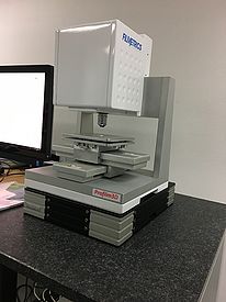
The Profilm3D optical profiler from Filmetrics uses white-light-interferometry (WLI) and phase-shifting-interferometry (PSI) to produce surface profiles and depth-of-field color images.
The main purpose is 3D topographic imaging of surfaces, step height measurements and roughness measurements with larger FOV (Field Of View) than the AFM, but less horisontal resolution.
For most samples the optical profiler provides fast and easy information without any sample preparation. However, it can be necessary to cover thin transparent layers (< 2 µm) with a thin layer of metal.
The resolution is limited by the objective and the sampling resolution.
The user manual, technical information and contact information can be found in LabManager:
Optical profiler (Filmetrics) info page in LabManager
| Equipment | Optical profiler | |
|---|---|---|
| Purpose | 3D topographic imaging of surfaces. |
|
| Posibilities | Interferometric profiling |
|
| Performance | With the current 10x objective | |
| Substrates | Substrate size |
|
| Substrate materials allowed |
| |
Dektak 3ST
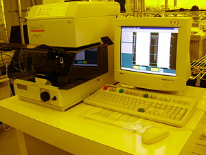
The Dektak 3ST is intended for profile measurements on samples outside the cleanroom.
The user manual, technical information and contact information can be found in LabManager:
Dektak 3ST (Dektak) in LabManager
The computer connected to the Dektak 3ST is pretty old and runs Windows 98 SE. It is not connected to the network but traces can be saved on either USB memory stick or floppy disk. The USB driver is an old universal driver and has been shown to work with small size USB sticks. However it did not work with an 8GB Kingston stick.
| Performance | Vertical Range |
|
|---|---|---|
| Scan length range |
| |
| Stylus track force |
| |
| Scan speed ranges |
| |
| Materials | Allowed substrate materials |
|
Stylus Profiler: Dektak150
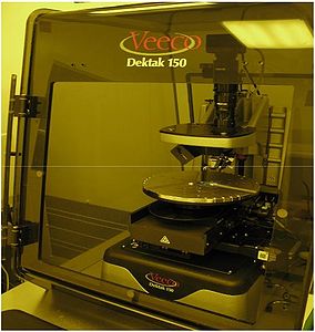
The stylus profiler Dektak150 is intended for profile measurements on samples outside the cleanroom.
The user manual, technical information and contact information can be found in LabManager:
Stylus profiler:Dektak150 in LabManager
The computer is not connected to the network but data can be saved on a dedicated USB and transfered to a computer on the network.
| Purpose | Profiler for measuring micro structures |
|
|---|---|---|
| Performance | Scan range x y |
Line scan x: 50 µm to 55 mm in a single scan |
| Scan range z |
50 Å to 1 mm | |
| Resolution x y |
Down to 0.003µm | |
| Resolution z |
1Å (@65kÅ), 10Å (@655 kÅ), 80 Å (@5240 kÅ), 160 Å (@1mm) | |
| Maximum sample thickness |
100mm | |
| Hardware settings | Tip radius |
|
| Substrates | Substrate size |
|
| Substrate materials allowed |
|

