Specific Process Knowledge/Etch/DRIE-Pegasus/FAQ/Nanoetch: Difference between revisions
Appearance
No edit summary |
No edit summary |
||
| Line 1: | Line 1: | ||
'''Feedback to this page''': '''[mailto:labadviser@nanolab.dtu.dk?Subject=Feed%20back%20from%20page%20http://labadviser.nanolab.dtu.dk/index.php/Specific_Process_Knowledge/Etch/DRIE-Pegasus/FAQ/Nanoetch click here]''' | |||
<!--Checked for updates on 2/10-2020 - ok/jmli --> | |||
<!--Checked for updates on 30/7-2018 - ok/jmli --> | <!--Checked for updates on 30/7-2018 - ok/jmli --> | ||
; Question | ; Question | ||
Revision as of 14:28, 2 October 2020
Feedback to this page: click here
- Question
- One of our 'popular' etches on the old ASE, a switched etch of nanostructures , is proving very difficult to transfer to the Pegasus. The structures are typically e-beam defined channels or holes a few hundred nanometers wide and masked with 50-100 nm ZEP resist. The etch load is usually very low, less than a few percent. We would like to go as much as 1 µm down. (I have been on paternity leave during the summer and I am sitting at home with my son right now so I don't have/know the complete story but I will get it for you if needed.) Do you have a suggestion to a starting point for such an etch?
- Answer
- Congratulations of your new addition! I can suggest a starting point for this but it would probably be best to wait until you can send me the additional details.
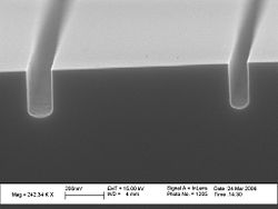
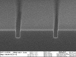
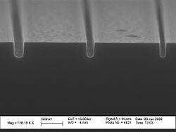
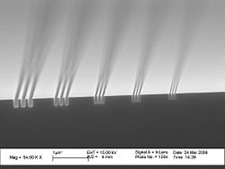
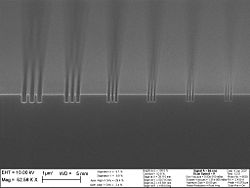
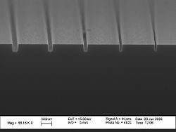
Three different examples of etch are shown here. The masking material was zep520A (80 nm).
- Question
- I have attached some images/summary of the nanoetches produced on the ASE and that we haven't been able to transfer to the Pegasus. What we are interested in is making small holes/trenches down to 30 nm diameter/width using ZEP520A E-beam resist as masking, hopefully as deep as 500 nm and (because of the small openings) with excellent selectivity. There is, in fact, a lot of need for this recipe so I really hope that you can help me with a starting point.
- Question
- Nano-scale etching on the Pegasus is relatively rare, however I would imagine that it should be possible to get similar results to those achieved in ICP. The process below was used to etch trenches of ~125nm to a depth of ~150nm with very low CD loss and smooth sidewall. The process was used to only etch a small amount to define the opening of the structure; following this a standard Bosch process was used to etch to several microns depth so we did not look at selectivity of this first opening step.
- 38SF6, 52C4F8, 4mT, 800W Coil, 50W platen, Platen @10°C, 38s to achieve 150nm depth.
- The process was run in long funnel configuration; if you are using short funnel, I would expect that a reduction of platen power would be needed but ultimately selectivity with long funnel is likely to be better.
- I will send the details on the positive profile etching shortly.

