Specific Process Knowledge/Characterization/XPS: Difference between revisions
No edit summary |
|||
| Line 6: | Line 6: | ||
==The XPS tools at DTU Nanolab== | ==The XPS tools at DTU Nanolab== | ||
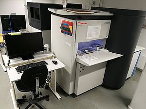
[[image:XPS K-Alpha.jpg | | [[image:XPS K-Alpha.jpg |300px|left| The XPS K-Alpha ]] | ||
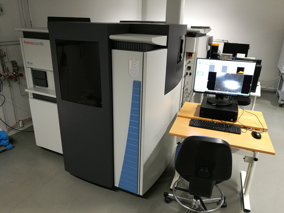
[[image:XPS Nexsa.png |300x300x|left| The XPS Nexsa ]] | [[image:XPS Nexsa.png |300x300x|left| The XPS Nexsa ]] | ||
Revision as of 17:12, 2 April 2020
Feedback to this page: click here
The XPS tools at DTU Nanolab


In the basement under the cleanroom two X-ray Photoelectron Spectroscopy (XPS) systems are installed in room 904. They are both manufactured by Thermofisher and they enable the users to perform elemental and chemical analysis of samples. The XPS K-Alpha is a base technique instrument providing XPS analysis. The XPS Nexsa is an upgraded version with all options.
Elemental analysis
The XPS instrument enables elemental analysis, chemical state analysis on the sample surface or deeper down by a depth profiling. A comparison about techniques and instruments used for elemental analysis at DTU Nanolab can be found on the page Element analysis.
More about the different possibilities of the XPS instrument is found here:
Getting access to the XPS tools
Click HERE to see information on how to get access to the XPS.
Analyzing XPS spectra
The analysis of XPS spectra is an art in itself. Click on the link below to find a some examples in which the Avantage software package has been used to extract information from experiments.
Techniques and option on the XPS tools
| Equipment | K-Alpha | Nexsa | |
|---|---|---|---|
| Purpose | Chemical analysis |
| |
| Performance | Spot size | Can be set between 30µm - 400µm | |
| Probing depth | Depending on probed element. Max probe depth lies within 10-200 Å. | ||
| Resolution | Dependent on probed elements. Concentrations down to about 0,5 atomic % can in some cases be detected. | ||
| Charge compensation |
Flood gun can be used for charge compensation of non conductive samples | ||
| Finding structures | Choose measuring spot from camera image (magnified) | ||
| Depth profiling | Purpose | With ion beam etch the top layer of the material can be removed, to do a depth profiling | |
| Ion beam size | About 3x1 mm | ||
| Substrates | Substrate size |
Maximum 60x60 mm | |
| Substrate thickness |
Maximum height about 20 mm | ||
