Specific Process Knowledge/Characterization/XRD/XRD SmartLab: Difference between revisions
| Line 27: | Line 27: | ||
!colspan="2" border="none" style="background:silver; color:black;" align="center"|Equipment | !colspan="2" border="none" style="background:silver; color:black;" align="center"|Equipment | ||
|style="background:WhiteSmoke; color:black"|<b>XRD SmartLab</b> | |style="background:WhiteSmoke; color:black"|<b>XRD SmartLab</b> | ||
|- | |- | ||
!style="background:silver; color:black;" align="center" width="60"|Purpose | !style="background:silver; color:black;" align="center" width="60"|Purpose | ||
| Line 44: | Line 43: | ||
*Roughness | *Roughness | ||
*Density | *Density | ||
|- | |- | ||
!style="background:silver; color:black" align="center" valign="center" rowspan="6"|X-ray generator | !style="background:silver; color:black" align="center" valign="center" rowspan="6"|X-ray generator | ||
| Line 54: | Line 50: | ||
|style="background:WhiteSmoke; color:black"| | |style="background:WhiteSmoke; color:black"| | ||
3 kW | 3 kW | ||
|- | |- | ||
|style="background:LightGrey; color:black"| | |style="background:LightGrey; color:black"| | ||
| Line 61: | Line 55: | ||
|style="background:WhiteSmoke; color:black"| | |style="background:WhiteSmoke; color:black"| | ||
20 to 45 kV | 20 to 45 kV | ||
|- | |- | ||
|style="background:LightGrey; color:black"| | |style="background:LightGrey; color:black"| | ||
| Line 68: | Line 60: | ||
|style="background:WhiteSmoke; color:black"| | |style="background:WhiteSmoke; color:black"| | ||
2 to 60 mA | 2 to 60 mA | ||
|- | |- | ||
|style="background:LightGrey; color:black"| | |style="background:LightGrey; color:black"| | ||
Type | Type | ||
|style="background:WhiteSmoke; color:black"| | |style="background:WhiteSmoke; color:black"| | ||
Sealed tube | Sealed tube | ||
| Line 80: | Line 68: | ||
|style="background:LightGrey; color:black"| | |style="background:LightGrey; color:black"| | ||
Target | Target | ||
|style="background:WhiteSmoke; color:black"| | |style="background:WhiteSmoke; color:black"| | ||
Cu | Cu | ||
| Line 89: | Line 75: | ||
|style="background:WhiteSmoke; color:black"| | |style="background:WhiteSmoke; color:black"| | ||
0.4 mm x 8 mm (Line/Point) | 0.4 mm x 8 mm (Line/Point) | ||
|- | |- | ||
!style="background:silver; color:black" align="center" valign="center" rowspan="5"|Goniometer | !style="background:silver; color:black" align="center" valign="center" rowspan="5"|Goniometer | ||
| Line 97: | Line 81: | ||
|style="background:WhiteSmoke; color:black"| | |style="background:WhiteSmoke; color:black"| | ||
incident / receiver coupled or independent | incident / receiver coupled or independent | ||
|- | |- | ||
|style="background:LightGrey; color:black"| | |style="background:LightGrey; color:black"| | ||
| Line 104: | Line 86: | ||
|style="background:WhiteSmoke; color:black"| | |style="background:WhiteSmoke; color:black"| | ||
300 mm | 300 mm | ||
|- | |- | ||
|style="background:LightGrey; color:black"| | |style="background:LightGrey; color:black"| | ||
| Line 111: | Line 91: | ||
|style="background:WhiteSmoke; color:black"| | |style="background:WhiteSmoke; color:black"| | ||
0.0001° (0.36") | 0.0001° (0.36") | ||
|- | |- | ||
|style="background:LightGrey; color:black"| | |style="background:LightGrey; color:black"| | ||
| Line 122: | Line 100: | ||
*X,Y:±50 mm for a 100 mm wafer | *X,Y:±50 mm for a 100 mm wafer | ||
*Rx,Ry:-5~+5° | *Rx,Ry:-5~+5° | ||
|- | |- | ||
|style="background:LightGrey; color:black"| | |style="background:LightGrey; color:black"| | ||
| Line 130: | Line 106: | ||
Diameter: 150 mm | Diameter: 150 mm | ||
Thickness: 0~21 mm | Thickness: 0~21 mm | ||
|- | |- | ||
!style="background:silver; color:black" align="center" valign="center" rowspan="2"|Optics | !style="background:silver; color:black" align="center" valign="center" rowspan="2"|Optics | ||
| Line 141: | Line 115: | ||
*Soller slit | *Soller slit | ||
*Variable divergence slit | *Variable divergence slit | ||
|- | |- | ||
|style="background:LightGrey; color:black"|Receiver side | |style="background:LightGrey; color:black"|Receiver side | ||
| Line 153: | Line 122: | ||
*Parallel slit analysers (PSA) | *Parallel slit analysers (PSA) | ||
*Ge(220)x2 analyser | *Ge(220)x2 analyser | ||
|- | |- | ||
!style="background:silver; color:black" align="center" valign="center" rowspan="3"|Substrates | !style="background:silver; color:black" align="center" valign="center" rowspan="3"|Substrates | ||
| Line 161: | Line 127: | ||
|style="background:WhiteSmoke; color:black"| | |style="background:WhiteSmoke; color:black"| | ||
up to 150 mm wafers | up to 150 mm wafers | ||
|- | |- | ||
| style="background:LightGrey; color:black"|Allowed materials | | style="background:LightGrey; color:black"|Allowed materials | ||
|style="background:WhiteSmoke; color:black"| | |style="background:WhiteSmoke; color:black"| | ||
All materials | All materials | ||
|- | |- | ||
|} | |} | ||
<br clear="all" /> | <br clear="all" /> | ||
Revision as of 16:12, 23 March 2020
XRD SmartLab
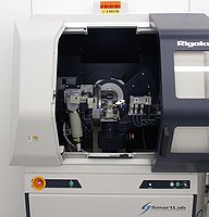
The Rigaku SmartLab is an advanced XRD for measuring on thin films. All thin films can be measured without fixating the sample, as the system has a so called In-Plane arm.

The user manual(s), user APV(s), technical information, and contact information can be found in LabManager:
Various measurement types including X-Ray reflectivity, Rocking curve, Theta-2theta, and Pole figures are described here:
Software for analysis
The software packages used for data analysis are available on the equipment computer, but we recommend that you install it on your personal computer. To run the software you need a USB dongle with a license on, these can be borrowed from the equipment responsible (in 2020, these were Kristian, Evgeniy, and Rebecca). We only have 9 dongles available, so when you are done please return the dongle to Nanolab.
The software can be found on "CleanroomDrive\_Equipment\XRD\Rigaku software\RILauncher", it should be possible to install the software without a dongle. To use the software you have to log in. The user is: Administrator. There is no password.
| Equipment | XRD SmartLab | |
|---|---|---|
| Purpose | Crystal structure analysis and thin film thickness measurement |
|
| X-ray generator |
Maximum rated output |
3 kW |
|
Rated tube voltage |
20 to 45 kV | |
|
Rated tube current |
2 to 60 mA | |
|
Type |
Sealed tube | |
|
Target |
Cu | |
|
Focus size |
0.4 mm x 8 mm (Line/Point) | |
| Goniometer |
Scanning mode |
incident / receiver coupled or independent |
|
Goniomenter radius |
300 mm | |
|
Minimum step size |
0.0001° (0.36") | |
|
Sample stage |
| |
|
Sample size |
Diameter: 150 mm Thickness: 0~21 mm | |
| Optics | Incident side |
|
| Receiver side |
| |
| Substrates | Substrate size |
up to 150 mm wafers |
| Allowed materials |
All materials | |
