Specific Process Knowledge/Etch/ICP Metal Etcher/silicon oxide: Difference between revisions
| Line 282: | Line 282: | ||
|-style="background:Black; color:White" | |-style="background:Black; color:White" | ||
!Results | !Results | ||
!Test on 6" wafer, by Peixiong Shi@ | !Test on 6" wafer, by Peixiong Shi@nanolab | ||
|- | |- | ||
|Etch rate of thermal oxide | |Etch rate of thermal oxide | ||
Revision as of 21:37, 25 November 2019
Feedback to this page: click here
It is possible to etch SiO2 in the ICP metal etcher but it is not designed for it and the results are not fantastic. It is a challenge to get a good selectivity to resist (typically in the range of 1:1 or worse) and it is probably not possible to get a profile angle of 90 degrees. More likely about 75-85 degrees. Different chemistries can be applied either based on CF4 or C4F8. If seems that C4F8 can give the best selectivity to resist (best case I have seem was 1:11 but it depends a lot on the process parameters)). If low coil power is needed CF4 chemistry is used because C4F8 needs a higher power to generate a plasma. /bghe 2016-04-25
Slow etch of SiO2 with resist as masking material - using a 6" carrier wafer with recess
This recipe can be used for slow etching of SiO2 with resist as masking material. Here are some test results presented.
| Parameter | Resist mask |
|---|---|
| Coil Power [W] | 200 |
| Platen Power [W] | 25 |
| Platen temperature [oC] | 0 |
| CF4 flow [sccm] | 20 |
| H2 flow [sccm] | 10 |
| Pressure [mTorr] | 3 |
SiO2 etch using DUV mask
Two chemistry regimes has been explored: One using CF4 and one using C4F8
- CF4: bad selectivity to the resist mask.
- C4F8: Better selectivity to the resist mask can be achieved
- Tests done by Peixiong
- Tests done by Berit
- Test by Zhibo Li @nanolab dec. 2016 - based on the work of Peixiong and Berit: File:Zhibo Li SiO2 ICP etch (dose205).docx
| Parameter | Recipe on ICP metal: A SiO2 etch with C4F8 with resist mask |
|---|---|
| Coil Power [W] | 1000 |
| Platen Power [W] | 200 |
| Platen temperature [oC] | 0 |
| C4F8 flow [sccm] | 10 |
| H2 flow [sccm] | 28 |
| Pressure [mTorr] | 2.5 |
| Results | Test |
|---|---|
| Etch rate of thermal oxide |
|
| Selectivity to resist [:1] | 4-5:1 (SiO2:resist) by bghe@nanolab (2015-06-02) |
| Cr etch rate | 1.6 nm/min (1:90 to SiO2) by Martin Lind Ommen (fall 2016) |
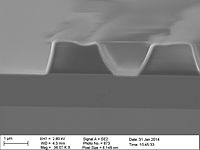
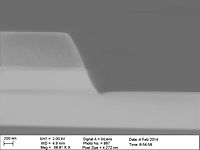
| Profile [o] | 86-87 dg by bghe@nanolab (2015-06-02) |
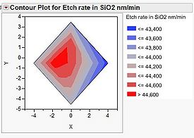
| Wafer uniformity map (click on the image to view a larger image) | |
| SEM profile images | 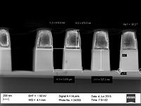 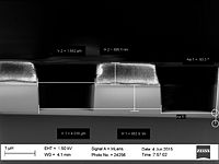 by bghe@nanolab (2015-06-02) |
| Etch rate in barc | |
| Etch rate in KRF resist | 34 nm/min by bghe@nanolab (2015-06-02) |
| Comments |
|
SiO2 etch nLOF
| Parameter | Resist mask |
|---|---|
| Coil Power [W] | 800 |
| Platen Power [W] | 100 |
| Platen temperature [oC] | 0 |
| CF4 flow [sccm] | 30 |
| H2 flow [sccm] | 10 |
| Pressure [mTorr] | 4 |
| Results | Test on wafer with 50% load (Travka 50), by BGHE @nanolab |
|---|---|
| Etch rate of thermal oxide | >110 nm/min (50% etch load) (09-03-2015) |
| Selectivity to resist [:1] | <0.7:1 (SiO2:resist) |
| Wafer uniformity (100mm) | Not known |
| Profile [o] | Not known |
| Wafer uniformity map (click on the image to view a larger image) | Not known |
| SEM profile images | NONE |
| Etch rate in nLOF resist | 1.6µm was removed after 10min |
| Comment | After 10min etch the resist was gone and the etch depth as 1.145µm in the oxide |
SiO2 etch with e-beam resist
| Process flow |
|---|
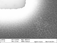
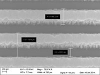
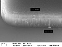
  px1283lablejan1542014t1  250uc
   at 40mm x y
  pxline400p1000jan142014dt2
  y=    -40    -45   -50   -55mm
  dose   200   240   280   320uc
|
| Parameter | Resist mask |
|---|---|
| Coil Power [W] | 800 |
| Platen Power [W] | 150 |
| Platen temperature [oC] | -10 |
| C4F8 flow [sccm] | 8 |
| H2 flow [sccm] | 30 |
| Pressure [mTorr] | 2.5 |
| Results | Test on 6" wafer, by Peixiong Shi@nanolab |
|---|---|
| Etch rate of thermal oxide | 131 nm/min (15-01-2014) |
| Selectivity to resist [:1] | ~1.8:1 (SiO2:resist) |
| Profile [o] | Not measured |
| Wafer uniformity map (click on the image to view a larger image) | Not known |
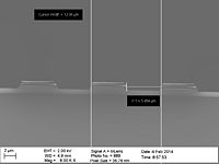
| SEM images |
|

