Specific Process Knowledge/Lithography/Descum: Difference between revisions
Appearance
| Line 40: | Line 40: | ||
===Plasma asher 2 === | ===Plasma asher 2 === | ||
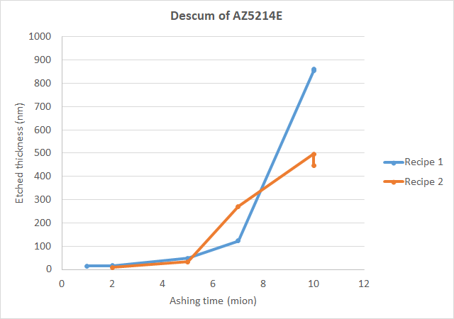
[[image:descum_graf.jpg|right|frame| | [[image:descum_graf.jpg|right|frame|355x355px|Descum results plasma asher 2]] | ||
Descum of AZ Mir 701 resist on 100mm silicon wafer. Five wafers were placed vertically in chamber. | Descum of AZ Mir 701 resist on 100mm silicon wafer. Five wafers were placed vertically in chamber. | ||
Revision as of 14:01, 22 November 2019
Feedback to this page: click here
Descum results
Plasma asher 1

Descum of AZ5214E resist on 50mm silicon wafer. Wafer was placed horisontally in chamber on a 100 mm carier wafer.
Note: Plasma asher was cold before use
| ||||||||||||||||||||||||||||||||||||||||||||||||||
Conny Hjort & Jesper Hanberg September 2019
Plasma asher 2

Descum of AZ Mir 701 resist on 100mm silicon wafer. Five wafers were placed vertically in chamber.
Experiment parameters:
|
|
