Specific Process Knowledge/Lithography/Descum: Difference between revisions
Appearance
| Line 71: | Line 71: | ||
| align="center" | | | align="center" | | ||
{| border="1" cellspacing="1" cellpadding="2" align="center" | {| border="1" cellspacing="1" cellpadding="2" align="center" | ||
! colspan=" | ! colspan="13" | Etched Thickness (nm) | ||
|- | |- | ||
! colspan="6" | ashing time (min) | ! colspan="6" | ashing time (min) | ||
|- style="background:LightGrey" | |- style="background:LightGrey" | ||
Revision as of 15:45, 19 November 2019
Feedback to this page: click here
Descum results
Plasma asher 1

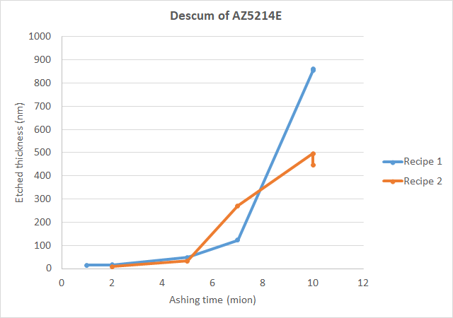
Descum of AZ5214E resist on 50mm silicon wafer. Wafer was placed horisontally in chamber on a 100 mm carier wafer.
Note: Plasma asher was cold before use

