Specific Process Knowledge/Lithography/Descum: Difference between revisions
Appearance
No edit summary |
|||
| Line 1: | Line 1: | ||
'''Feedback to this page''': '''[mailto:photolith@danchip.dtu.dk?Subject=Feed%20back%20from%20page%20http://labadviser.danchip.dtu.dk/index.php?title=Specific_Process_Knowledge/Lithography/Descum click here]''' | |||
<!-- Replace "http://labadviser.danchip.dtu.dk/..." with the link to the Labadviser page--> | |||
==Descum results== | ==Descum results== | ||
| Line 26: | Line 29: | ||
|- | |- | ||
|} | |} | ||
Conny Hjort & Jesper Hanberg | |||
September 2019 | |||
Revision as of 16:41, 21 October 2019
Feedback to this page: click here
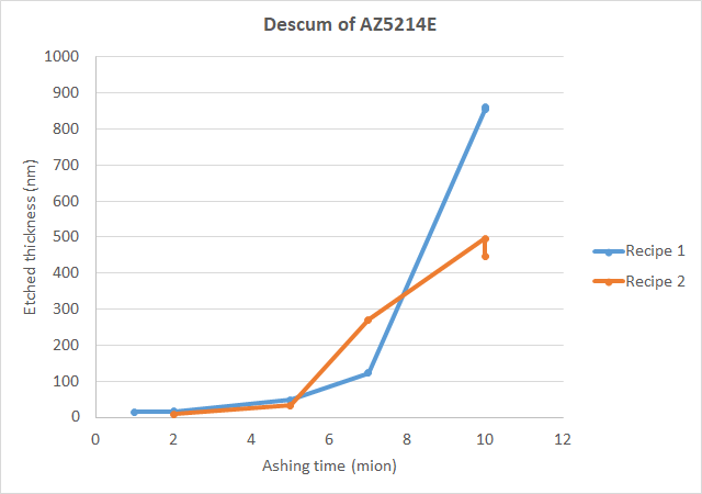
Descum results
Plasma asher 1

Descum of AZ5214E resist on 50mm silicon wafer. Wafer was placed horisontally in chamber on a 100 mm carier wafer.
Note: Plasma asher was cold before use
Conny Hjort & Jesper Hanberg September 2019 |
||||||||||||||||||||||||||||||||||||||||||||||||||
