Specific Process Knowledge/Thermal Process/Jipelec RTP: Difference between revisions
Appearance
| Line 25: | Line 25: | ||
|style="background:LightGrey; color:black"|Process Temperature | |style="background:LightGrey; color:black"|Process Temperature | ||
|style="background:WhiteSmoke; color:black"| | |style="background:WhiteSmoke; color:black"| | ||
*0- | *0-1100 <sup>o</sup>C | ||
*III-V materials only to 450 <sup>o</sup>C | *III-V materials only to 450 <sup>o</sup>C | ||
*Temperature ramp up to 300 <sup>o</sup>C/min | *Temperature ramp up to 300 <sup>o</sup>C/min | ||
| Line 35: | Line 35: | ||
*Vacuum | *Vacuum | ||
|- | |- | ||
|style="background:LightGrey; color:black"| | |style="background:LightGrey; color:black"|Gases on the system | ||
|style="background:WhiteSmoke; color:black"| | |style="background:WhiteSmoke; color:black"| | ||
| Line 43: | Line 43: | ||
|style="background:LightGrey; color:black"|Batch size | |style="background:LightGrey; color:black"|Batch size | ||
|style="background:WhiteSmoke; color:black"| | |style="background:WhiteSmoke; color:black"| | ||
*One 100 mm wafer | *One 50 mm or 100 mm wafer | ||
*Small samples (placed on a carbide carrier or a Si carrier wafer with 1 µm oxide) | *Small samples (placed on a carbide carrier or a Si carrier wafer with 1 µm oxide) | ||
|- | |- | ||
| style="background:LightGrey; color:black"|Substrate | | style="background:LightGrey; color:black"|Substrate materials allowed | ||
|style="background:WhiteSmoke; color:black"| | |style="background:WhiteSmoke; color:black"| | ||
A silicon carrier wafer with 1 µm oxide is | A carrier is always needed: For III-V materials a carbide carrier is used, and for other samples a silicon carrier wafer with 1 µm oxide is used | ||
*Silicon | *Silicon | ||
*Silicon | *Silicon oxide | ||
*Silicon | *Silicon nitride | ||
* | *Fused silica/quartz | ||
*Polysilicon | *Polysilicon | ||
*III-V materials (on graphite carrier, max 450 <sup>o</sup>C) | |||
*III-V materials (on graphite carrier) | *Some metals - Ask the Thin Film group for permission | ||
* | |||
|- | |- | ||
|} | |} | ||
Revision as of 10:19, 1 April 2019
Feedback to this page: click here
Jipelec - Rapid Thermal Processing

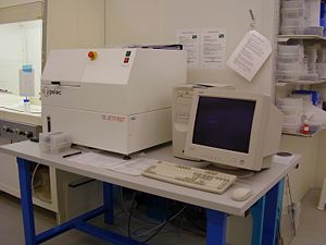
The Jipelec is a rapid thermal processing (RTP) oven. It is be used for fast and well-controlled annealing or alloying of samples. It is possible to use either a thermocouple or a pyrometer to control the temperature (of the sample carrier).
The user manual, technical information and contact information can be found in LabManager:
| Purpose | RTP annealing | |
|---|---|---|
| Process parameter range | Process Temperature |
|
| Process pressure |
| |
| Gases on the system |
| |
| Substrates | Batch size |
|
| Substrate materials allowed |
A carrier is always needed: For III-V materials a carbide carrier is used, and for other samples a silicon carrier wafer with 1 µm oxide is used
|
