Specific Process Knowledge/Thermal Process/C4 Aluminium Anneal furnace: Difference between revisions
Appearance
| Line 28: | Line 28: | ||
|style="background:WhiteSmoke; color:black"| | |style="background:WhiteSmoke; color:black"| | ||
*Annealing of wafers with aluminium | *Annealing of wafers with aluminium | ||
|- | |- | ||
!style="background:silver; color:black" align="center" valign="center" rowspan="3"|Process parameter range | !style="background:silver; color:black" align="center" valign="center" rowspan="3"|Process parameter range | ||
| Line 42: | Line 41: | ||
|style="background:WhiteSmoke; color:black"| | |style="background:WhiteSmoke; color:black"| | ||
*N<sub>2</sub>: 0-10 slm | *N<sub>2</sub>: 0-10 slm | ||
|- | |- | ||
!style="background:silver; color:black" align="center" valign="center" rowspan="2"|Substrates | !style="background:silver; color:black" align="center" valign="center" rowspan="2"|Substrates | ||
| Line 52: | Line 50: | ||
|style="background:WhiteSmoke; color:black"| | |style="background:WhiteSmoke; color:black"| | ||
*Silicon wafers with aluminium. | *Silicon wafers with aluminium. | ||
Silicon wafers with ALD oxides | *Silicon wafers with ALD oxides Al2O<sub>3<{sub> and TiO<sub>2</sub> | ||
*Wafers are allowed enter the furnace after aluminium lift-off or after aluminium etch and resist strip in acetone | *Wafers are allowed enter the furnace after aluminium lift-off or after aluminium etch and resist strip in acetone | ||
|- | |- | ||
|} | |} | ||
Revision as of 12:53, 28 March 2019
Feedback to this page: click here
Aluminium Anneal furnace (C4)

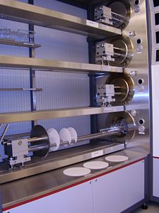
The Aluminium Anneal furnace (C4) is a Tempress horizontal furnace for annealing of silicon wafers with aluminium or ALD oxides Al2O3 and TiO2.
This furnace is the lowest of the furnace tubes in the furnace C-stack positioned in cleanroom B-1. In this furnace allowed to process wafers that contain aluminium. Please check the cross contamination information in LabManager before you use the furnace.
The user manual, technical information and contact information can be found in LabManager:
Process knowledge
- Annealing: look at the Annealing page
| Purpose |
| |
|---|---|---|
| Process parameter range | Process Temperature |
|
| Process pressure |
| |
| Gas flows |
| |
| Substrates | Batch size |
|
| Substrate materials allowed |
|
