Specific Process Knowledge/Etch/Etching of Silicon/Si etch using ASE: Difference between revisions
No edit summary |
|||
| Line 145: | Line 145: | ||
== Process development == | == Process development == | ||
===Etch of nano sized structures=== | ===Etch of nano sized structures=== | ||
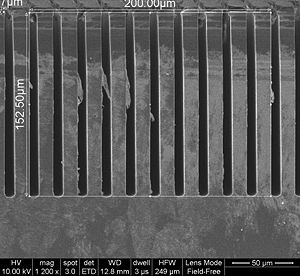
Three different examples of etch are shown here. The masking material was zep520A (80 nm). | |||
Revision as of 14:00, 1 December 2008
The Bosch process: Etching of silicon
The Bosch process uses alternation between an etch cycle and a passivation cycle. Introducing a passivation step in an etch process is very beneficial for the control of the angle of the sidewalls in the etch process because it allows us to cover them with a protective layer that suppresses the isotropic etching. Combined with the high plasma density in the ICP chamber, the excellent sidewall control enables us to etch high aspect ratio structures in silicon with very high etch rates.
In the case of the silicon etching on the ASE, an etch phase with SF6 and O2 alternates with a passivation phase with C4F8.
The two standard silicon etch recipes
Two recipes have been optimized for the ASE. Their specification is on a 10 % etch load wafer with trenches.
- Shallolr: The shallow etch process will etch a 2 m opening down to make a 20 m trench.
- Deepetch: The deep etch process will etch a 50 m opening down to make a 300 m trench.
The standardization procedure on the ASE covers these two etches.
Recipes on the ASE
Shallolr
The shallolr recipe is designed to etch features (with sizes above 1 m) in silicon down to a depth that ranges from a few microns to some 50 microns. (If you need to etch deeper use Deepetch or more shallow, see Nanoetches.) It is specified to etch a 2 m wide trench down to a depth of 20 m on a wafer that has a global/local etch opening density of 10%.
The recipe is given below.
| Common parameters | Multiplexed parameters | |||
|---|---|---|---|---|
| Parameter | Setting | Parameter | Etch | Passivation |
| Temperature | 10oC | SF6 Flow | 260 sccm | 0 sccm |
| No. of cycles | 31 | O2 Flow | 26 sccm | 0 sccm |
| Process time | 5:56 mins | C4F4 Flow | 0 sccm | 120 sccm |
| APC mode | manual | RF coil | 2800 W | 1000 W |
| APC setting | 86.8 % | RF Platen | 16 W | 0 W |
| Cycle time | 6.5 s | 5 s | ||
The process runs for 31 cycles (5:56 mins). The fact that it's Bosch process is clear from the scallops on the sidewalls - one should be able to count 31 of them.
- Standardization images of the shallolr recipe
-
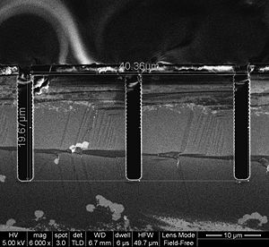 The profile of a 2 m trench
 -
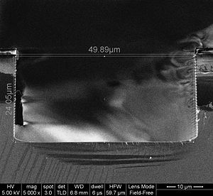 The profile of a 50 m trench


The process is designed to reach 20 m down in a 2 m trench but as is clear from the image of the corresponding 50 m trench, this one is etched deeper. The reason is the so called Aspect Ratio Dependent Etching or ARDE: See below.
Deepetch
The deepetch recipe is designed to etch features (with sizes 2 m) in silicon down to a depth that ranges from some 50 microns to hundreds of microns. (If you need to etch less, use shallow or Nanoetches.) It is specified to etch a 50 m wide trench down to a depth of 300 m on a wafer that has a global/local etch density of 10%.
The recipe is given below.
| Common parameters | Multiplexed parameters | |||
|---|---|---|---|---|
| Parameter | Setting | Parameter | Etch | Passivation |
| Temperature | 20oC | SF6 Flow | 230 sccm | 0 sccm |
| No. of cycles | 250 | O2 Flow | 23 sccm | 0 sccm |
| Process time | 54:10 mins | C4F4 Flow | 0 sccm | 120 sccm |
| APC mode | manual | RF coil | 2800 W | 1000 W |
| APC setting | 87.7 % | RF Platen | 19 W | 0 W |
| Cycle time | 8 s | 5 s | ||
- Standardization images of the deepetch recipe
-
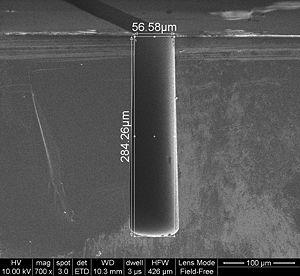
 The profile of a 2 m trench
 -
 The profile of a 50 m trench


As is clear from the two images ARDE also plays a role in this case: The 2 m trench (widened to about 5-6 m because of undercut/underetching) is only etched 150 m.
Standardization procedure on the ASE
Process development
Etch of nano sized structures
Three different examples of etch are shown here. The masking material was zep520A (80 nm).