
Specific Process Knowledge/Thin film deposition/Deposition of Gold/Adhesion layers: Difference between revisions
No edit summary |
|||
| Line 36: | Line 36: | ||
To avoid oxidation of Ti or Cr that is in physical contact with the nano-electronic materials, one solution is to avoid these materials completely. Indeed, some of the best performing CNT devices are made without the use of adhesion layers, as e.g. Pd which is directly used. '''If an adhesion layer is required for mechanical stability, a less than 2nm thin Cr layer is recommended and Ti must be avoided'''. This is because the partially oxidized Ti might form a barrier between the nano-electronic material and the Au over-layer, with a consequent deterioration of the electron transport performances. Because of the single-layer morphology due to the Cr-Au alloy formation, the alloy will make electrical and physical contact to the nano-electronic material, despite the chrome oxide content. Furthermore, a low temperature annealing will enhance inter-diffusion of Au and Cr and improve electrical contact between the nano-electronic material and the Au over-layer. | To avoid oxidation of Ti or Cr that is in physical contact with the nano-electronic materials, one solution is to avoid these materials completely. Indeed, some of the best performing CNT devices are made without the use of adhesion layers, as e.g. Pd which is directly used. '''If an adhesion layer is required for mechanical stability, a less than 2nm thin Cr layer is recommended and Ti must be avoided'''. This is because the partially oxidized Ti might form a barrier between the nano-electronic material and the Au over-layer, with a consequent deterioration of the electron transport performances. Because of the single-layer morphology due to the Cr-Au alloy formation, the alloy will make electrical and physical contact to the nano-electronic material, despite the chrome oxide content. Furthermore, a low temperature annealing will enhance inter-diffusion of Au and Cr and improve electrical contact between the nano-electronic material and the Au over-layer. | ||
= | = Characterization of adhesion layer effect on Au thin films = | ||
== Effect on Au film morphology, grain size and texture == | == Effect on Au film morphology, grain size and texture == | ||
Revision as of 13:45, 30 August 2018
Feedback to this page: click here
This work was performed by PhD student Matteo Todeschini during period 2014-2017
Adhesion layers
The deposition of metal thin-film structures on dielectric or semiconductor substrates is important in a wide range of micro/nanofabrication applications (plasmonics, metamaterials, organic transistors, substrates for graphene growth, field effect devices).
Noble metals such as Au, Ag, and Pt are often used for the fabrication of these structures. Noble metals are preferred for their high thermal and electrical conductivities, strong and unique optical resonances in the visible and near-infrared (NIR) region of the electromagnetic spectrum due to the resonant response of their free electrons to the electric field of light, and chemical inertness. However, their chemical inertness is also a problem during the fabrication process, because the layers adhere poorly to the substrate, leading to different phenomena like delamination, peeling and deterioration of device performance over time.
An empiric approach has been applied to the adhesion enhancement, leading to the application of extremely thin adhesion layers between the substrate and the noble metal films. The most used of these adhesion layers are transition metals like Ti and Cr, but the advantages of using these materials as adhesion layers are poorly understood.
Fig. 1 represents the simplified adhesion layer model usually used in the micro and nanofabrication community for a generic bilayer system. In this model, the adhesion layer and the noble metal over-layer are deposited sequentially by PVD and are considered to be completely uniform and in perfect contact. Ti and Cr are known to be more chemically reactive than noble metals and thereby increase the adhesion as they chemically bind to the substrate. However, the model does not include any layer-layer interaction. Moreover, it is considered to be independent of the thin-film thickness. Due to the continuous miniaturization of structures and devices, the total metal thin-film thicknesses have reached tens of nanometers, with the thickness of the over-layer approaching the one of the adhesion layer. In these conditions it is unclear if the simplified model is still adequate.

Here the first recommendations on the adhesion layers best suited for specific nanodevice applications are presented. Below the background and characterization work carried out on two main thin-film systems, Cr/Au and Ti/Au stacks, to arrive at these recommendations is presented.
Recommendations for nanodevice fabrication
Nano-optic devices
For nano-optic devices there are two implications:
1) the grain size values of the Au thin-films are comparable with the sizes of plasmonic nanostructures, which are 70-200 nm. Hence, each nanostructure might have multi-grain structures that are different. This might affect its interaction with the light and its optical response, which leads to broadening of the optical resonance peaks.
2) during light and plasmonics device interactions, the temperature can locally raise to above 795 K, further enhancing the alloying of Cr and Au already present at room temperature and thus deteriorating the electrical properties of the thin-film stack.
Ti does not inter-diffuse with Au at room temperature, supported by the µ4PP measurements which show that the electrical properties appear to be similar to pure Au thin-films. The formation of a stable Ti layer under the Au prevents diffusion of Au into the underlying substrate and improves the performance-time and temperature stability of the devices. The Ti-Au inter-diffusion starts at temperatures higher than 175°C. If the devices have to be used for prolonged time above this temperature, Pd and Pt diffusion barriers must be used. Comparative studies show a localized surface plasmon damping in plasmonic nanostructures due to the presence of a very thin adhesion layer, and overall better performances of Ti over Cr for the optical resonance of such nanostructures.
Therefore, if the choice is limited to metallic adhesion layers, Ti is preferred over Cr for nano-optics applications. A perhaps even better alternative is to use organosilane-based adhesion layers. Comparative measurements of Ti vs Mercaptopropyltrimethoxysilane (MPTMS) and Cr vs Aminopropyltrimethoxysilane (APTMS) show overall better performances for the organosilane-based adhesion layers over the metallic ones. A considerable disadvantage of these molecular adhesion layers is their lack of compatibility with the lithographic and lift-off processes, which still play an important role in the fabrication of nanostructures.
Nano-electronic devices
For nano-electronics applications, the reported results show that Ti and Cr form oxides with surface adsorbed water and free oxygen in the vacuum chamber of the physical vapor deposition system. To avoid oxidation of the adhesion layer, the chamber vacuum needs to be in UHV conditions and the sample must be baked to remove the surface adsorbed water. However, these baking temperatures are not compatible with e.g. lift-off nanofabrication of nano-electronic devices that often utilize photo- or electron beam lithography resists which do not tolerate high baking temperatures.
To avoid oxidation of Ti or Cr that is in physical contact with the nano-electronic materials, one solution is to avoid these materials completely. Indeed, some of the best performing CNT devices are made without the use of adhesion layers, as e.g. Pd which is directly used. If an adhesion layer is required for mechanical stability, a less than 2nm thin Cr layer is recommended and Ti must be avoided. This is because the partially oxidized Ti might form a barrier between the nano-electronic material and the Au over-layer, with a consequent deterioration of the electron transport performances. Because of the single-layer morphology due to the Cr-Au alloy formation, the alloy will make electrical and physical contact to the nano-electronic material, despite the chrome oxide content. Furthermore, a low temperature annealing will enhance inter-diffusion of Au and Cr and improve electrical contact between the nano-electronic material and the Au over-layer.
Characterization of adhesion layer effect on Au thin films
Effect on Au film morphology, grain size and texture
From the cross section profile of the 2nm Au sample (Fig. 2a), it is clear that Au, when deposited directly on SiO2, in order to reduce the interface energy, forms a nanoparticle-like layer in contrast to a continuous film. The diameter of the nanoparticles is about 10 nm. The nanoparticle morphology is confirmed by AFM analysis (Fig. 2b). The RMS surface roughness was measured to be 2.4 nm. For comparison, the RMS roughness of the SiO2 substrate was 0.3 nm. When the thin-film nominal thickness is increased to 20 nm (20nm Au sample, Fig. 2c), the Au layer becomes continuous, but a certain degree of surface roughness is still present due to grain coalescence. The AFM image (Fig. 2d) shows an RMS surface roughness of 1.0 nm, which is significantly lower than the 2nm Au sample.

From the TEM bright field cross section analysis of the 2nm Ti/2nm Au sample, it is observed that 2 nm of Ti forms a continuous layer below the Au layer (Fig. 3a). The Au layer is continuous over the Ti, indicating that Ti is responsible for an interface energy decrease, acting as an adhesive. The AFM analysis of the same sample confirmed the continuous structure, and an RMS surface roughness of 0.8 nm was measured (Fig. 3b). The 2nm Ti/20nm Au sample also shows a smoother film compared to the 20nm Au sample (Fig. 3c), and the AFM analysis shows an RMS surface roughness of 0.5 nm (Fig. 3d), very similar to the one of the Si substrate.
In contrast to the case with the Ti adhesion layer, TEM bright field analysis of the 2nm Cr/2nm Au sample shows a single continuous layer (Fig. 4a). The AFM RMS surface roughness is 1.2 nm (Fig. 4b). Increasing the nominal Au thickness to 20 nm for the 2nm Cr/20nm Au sample, the film still presented a single-layer morphology (Fig. 4c), while the RMS surface roughness decreased to 0.6 nm (Fig. 4d).
-
 Fig. 3: TEM cross section images and 300x300 nm AFM images of the 2nm Ti/2nm Au sample (a-b) and of the 2nm Ti/20nm Au sample (c-d).
 -
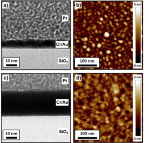 Fig. 4: TEM cross section images and 300x300 nm AFM images of the 2nm Cr/2nm Au sample (a-b) and of the 2nm Cr/20nm Au sample (c-d).


To investigate the crystal orientation of the metal thin-films, tramsimission Kikuchi diffraction was used (Fig. 5a) (see Transmission Kikuchi diffraction for more information). The nanostructure of the 20nm Au film has a bimodal grain size distribution (Fig. 5b). While the smaller grains have different crystal orientations, the large grains (blue color) all have [111] orientation.
Microstructural evolution and growth of metal thin-films deposited by physical vapor deposition on amorphous dielectric substrates follows island growth. The first thin-film growth step is the nucleation of small islands once the activation barrier and the critical nuclei size have been overcome. It is followed by a second step of island growth, during which the impinging atoms contribute to increase island size. The third step, usually happening simultaneously with step 2, is island coalescence, where a strong driving force is present for coarsening through surface atom diffusion and grain boundaries (GB) motion. During this process, the island growth is driven by the minimization of surface and interface energy.
Fig. 6a represents two Au islands having different crystal orientations. In particular they have the (111)- and (100)-facets, respectively, parallel to the substrate surface. The growth of these islands is dependent on their orientation (Fig. 6b): for Au, which has a face-centered cubic unit cell, the (100) surface has a higher surface energy than the (111) surface, and to minimize energy, the (100) surface grows faster. Islands having (100) or (110) facets parallel to the substrate grow faster in the vertical direction, while islands with (111) facets parallel to the substrate grow faster laterally. The result is a continuous film, having laterally larger and flatter islands with [111] crystal direction, and laterally smaller but taller islands with [100] and [110] orientations.
-
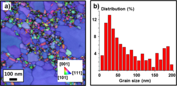 Fig. 5: TKD inverse pole figure z-direction (IPFZ) map of the growth direction (a) and grain size distribution (b) of the 20nm Au sample.
 -
![Fig. 6: (a) Schematic representation of [111] and [100] Au islands on a SiO2 substrate. The crystal direction is referred parallel to the substrate surface. (b) Representation of the orientation-driven growth of the islands on the substrate: the {100} facets grow faster than {111} ones in order to decrease surface energy.](/images/thumb/9/94/Picture3.png/350px-Picture3.png) Fig. 6: (a) Schematic representation of [111] and [100] Au islands on a SiO2 substrate. The crystal direction is referred parallel to the substrate surface. (b) Representation of the orientation-driven growth of the islands on the substrate: the {100} facets grow faster than {111} ones in order to decrease surface energy.
Fig. 6: (a) Schematic representation of [111] and [100] Au islands on a SiO2 substrate. The crystal direction is referred parallel to the substrate surface. (b) Representation of the orientation-driven growth of the islands on the substrate: the {100} facets grow faster than {111} ones in order to decrease surface energy.

![Fig. 6: (a) Schematic representation of [111] and [100] Au islands on a SiO2 substrate. The crystal direction is referred parallel to the substrate surface. (b) Representation of the orientation-driven growth of the islands on the substrate: the {100} facets grow faster than {111} ones in order to decrease surface energy.](/index.php?title=File:Picture3.png)
The samples with the adhesion layers and 20 nm Au layer were also analyzed. The addition of the adhesion layer had in both cases a profound impact on grain size and orientation of the Au film, as visible in Fig. 7a and 7c. The image shows small grains mainly oriented in the [111] crystal direction, with an average grain size of 40 nm for Ti (Fig. 7b) and 36 nm for Cr (Fig. 7d). During the collection of the TKD maps, only the Kikuchi patterns produced by the electron scattering from the Au layer were recorded and indexed. Cr and Ti layers did not contribute to the pattern formation due to two main reasons: i) they are too thin to produce enough scattered electrons and ii) they are worse electron scattering centers tahn Au because they have a lower atomic number.

The smaller grain size is attributed to an enhanced wetting of the deposited Au promoted by the adhesion layer. The enhanced wetting behaviour increases the number of nucleation sites compared to the pure Au film case, where Au is evaporated directly onto the SiO2 surface. This eventually leads to a much denser nucleation of the Au grains, which at the same time facilitates the inter-diffusion of Au atoms. The enhanced wetting might be due to the formation of Ti-Au and Cr-Au bonds.
The very dominant [111] crystal orientation observed implies a decrease of the energy barrier for the formation of the energetically most favourable Au crystal structure. This is promoted by the denser nucleation and stronger inter-diffusion of Au atoms described above. In contrast to the pure Au case, all the grains have the same diffusion rate of the (111) exposed planes, and therefore the grains grow with a narrow grain size distribution. Since the film has been deposited at room temperature, the system did not have enough energy to overcome the energy barrier for grain coalescence, hence resulting in grains with a small average size. For the Cr case, also small grains with [100] and [110] crystal orientations were detected. This might suggest that for Au on Cr the [111] orientation is energetically less favored with respect to the [100] and [110] orientations compared to the Ti/Au case.
Bilayer chemical composition and elemental distribution
The knowledge of the chemical composition and elemental distribution of the bilayer systems is important to understand the type of interaction between the layers and their different structure. To obtain such information, the bilayer systems were investigated using STEM-EDX, STEM-EELS and XPS depth profiling.
For the chemical distribution of the elements in the 2nm Ti/2nm Au sample, the STEM-EDX measurements at the Ti/Au interface showed the presence of a continuous Ti layer below the Au layer (Fig. 8a). The analysis of the 2nm Cr/2nm Au sample showed instead the presence of Cr throughout the whole thickness of the Au layer (Fig. 8b). Since Cr and Au were deposited sequentially and not by a co-deposition process, this result suggests a strong inter-diffusion. The 2nm Cr/20nm Au sample was also investigated, to understand the degree of inter-diffusion for a thicker Au layer (Fig. 8c). In this case the inter-diffusion between the elements was incomplete, being present for a thickness of 2-3 nm. This suggests that the diffusion process is limited to such a thickness when Cr and Au are deposited at room temperature.
To verify the chemical composition of the samples, in particular to investigate a possible presence of oxygen in the adhesion layer, STEM-EELS analysis was used. A line scan across the layer interfaces of the 2nm Ti/2nm Au sample shows the presence of a Ti core loss L3 edge at 460 eV and an L2 edge at 465 eV. A SiO2 O-K edge is visible at 538 eV, while the O-K edge of O bounded to Ti is found at 532 eV (Fig. 9a). The same investigation was performed on the 2nm Cr/2nm Au sample (Fig. 9b). The analysis showed a Cr L3 edge at 585 eV and an L2 edge at 594 eV. The SiO2 O-K edge is visible at 545 eV, while at 540 eV a weak OCr-K edge of O bounded to Cr is visible for a limited thickness below Au. Furthermore, the Cr edge presents a compositional tail along the scan direction, which confirms diffusion into the Au layer. For the length of the tail there is no presence of OCr-K edge, indicating that Cr inside Au is in metallic form. This is in good agreement with the observed diffusion, which involves only metallic Cr.
-
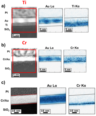 Fig. 8: STEM-EDX maps of the 2nm Ti/2nm Au sample (a), 2nm Cr/2nm Au sample (b) and 2nm Cr/20nm Au sample (c). The Au L-alpha signal is acquired at 9713 eV, the Ti K-alpha signal at 4510.9 eV and the Cr K-alpha signal at 5414.7 eV.
 -
 Fig. 9: (a) STEM-EELS linear scan of the 2nm Ti/2nm Au sample, showing the presence of oxygen in the Ti layer. (b) STEM-EELS linear scan of the 2nm Cr/2nm Au sample, which shows the presence of oxygen that is bounded to Cr and Cr diffusion into the Au layer.


The source of oxidation of the adhesion layer could have three origins: i) oxidation due to migration of oxygen from the SiO2 substrate, ii) oxidation during the e-beam deposition process, or iii) oxidation due to substrate contamination with water and oxygen molecules. To investigate the oxidation origin, XPS depth profile analysis were performed on 2nm Ti/20nm Au and 2nm Cr/20nm Au as-deposited samples.
The first analysis was performed to clarify if oxygen was originating from source i). To rule out possible oxygen migration from the oxygen-rich SiO2 substrate, the metal thin-films were deposited on amorphous Si3N4. For both samples, after Ar ion milling of 20 nm of Au, the Au 4f signal intensity decreased and Cr 2p and Ti 2p signals started to appear together with the O 1s signal (Fig. 10a for Ti and 10b for Cr, respectively).

Peak fits for the Ti and Cr signals were performed, and are reported in Fig. 11. The Ti 2p peak is a convolution of three components: a TiN doublet at 455.0 and 461.1 eV, a TiO2 doublet at 457.7 and 464.0 eV and a TiOx signal, which forms the descending background tail. The fit gives the following information: 1) Ti has formed Ti-N bonds with the Si3N4 substrate; 2) the adhesion layer was partially oxidized during deposition and not from source i). Metallic Ti could not be detected, but its presence cannot be excluded: metallic Ti is highly reactive with respect to oxygen and nitrogen, and the destructive sputtering process used for the depth profiling could have enhanced the mixing between Ti, O and N, catalyzing the reaction of the metallic Ti bound to Au to form an oxide or a nitride. The Cr 2p peak fit is formed by three components: a metallic Cr doublet at 574.4 and 583.6 eV, a Cr2O3 doublet at 576.3 and 585.6 eV and a CrO3 doublet at 580 and 589.2 eV. The result of the fit indicates a partial oxidation of Cr, as in the Ti case.

The second analysis was performed to understand whether the oxygen was originating from source ii) or iii). A 2nm Ti/20nm Au/2nm Ti/20nm Au sandwich structure was deposited and analyzed. Both layers of Ti were partially oxidized: the Ti 2p peak signals (Fig. 12a) are present at the same depth together with the O 1s signals (Fig. 12b). The O 1s signal in the Ti layer in contact with the Si3N4 substrate has higher intensity than the one of the Ti layer between the Au layers. Hence, the Ti layer in contact with the substrate is more oxidized, which suggests that Ti reacted with water adsorbed on the substrate surface. The conclusion is that the oxygen originated from oxidation during the e-beam deposition process and from oxidation due to substrate contamination with water and oxygen molecules.

Adhesion layer effect on bilayer thin-film electrical resistivity
The change in nanostructure of the Au thin film due to the presence of the adhesion layers observed above, could have an important impact on the film macroscopic properties such as electrical resistivity. Electrical resistivity in polycrystalline films is dependent on electron scattering at surfaces and grain boundaries, and it was expected that the grain size change measured with TKD to be reflected in the electrical properties. Furthermore, for the case of Cr, a Cr-Au alloy was formed, which also was expected to have an impact on the thin-film electrical resistivity.
To verify these hypotheses, the sheet resistance (R) of the three samples (20nm Au, 2nm Ti/20nm Au, and 2nm Cr/20nm Au) was measured using micro 4-point probe (µ4PP). Fig. 13a shows that the Ti/Au sample had a lower sheet resistance than pure Au, which can be attributed to the two layers acting as parallel resistors. Data normalization was performed with respect to the average sheet resistance (R) measured at the 20-Au sample. To exclude tip wear effects of the µ4PP, the measurements were performed measuring with the same probe alternatively on the 20nm Au and 2nm Ti/20nm Au sample, respectively. Fig. 13b shows that the Cr/Au system had a higher sheet resistance than pure Au. In this case, the formation of a single layer due to Cr-Au inter-diffusion compromised the multilayer assumption. The sheet resistance increase is in line with the general resistivity increase of Cr-Au alloys, which increases linearly with the Cr concentration. Data acquisition and normalization were done as in the Ti/Au case.
The Ti/Au parallel behavior and Cr/Au inter-diffusion seem to have a larger impact on the electrical properties of the multilayer systems than the nanostructure change observed by TKD. For both samples, the increase of grain boundary scattering due to the higher density of grain boundaries, compared to pure Au, could not be measured with setup used, but cannot be excluded a priori.

Adhesion layer model
Based on the results obtained above, a revised adhesion layer model for Ti/Au and Cr/Au thin-film systems is proposed. The model is intended as an improvement in the description of the layer-layer interaction compared to the model described in Fig. 1, with the aim of helping the thin-film engineering of nanodevices.
The adhesion layer model is shown in Fig. 14. The growth of both adhesion layers starts with the deposition of the atoms on the substrate (1) and the subsequent formation of an amorphous layer (2). During the deposition, both Ti and Cr get partially oxidized by oxygen and water molecules present on the substrate surface and in the deposition chamber. The adhesion layer acts as a wetting layer for Au, reducing the nucleation energy barrier and increasing the number of nucleation sites compared to the case where Au is directly evaporated onto the SiO2 surface. The enhanced wetting is due to the formation of Ti-Au and Cr-Au chemical bonds. This leads to the formation of a continuous film having i) monodisperse grain size and ii) the energetically most favorable [111] crystal orientation for Au (3). For the Cr/Au system there is an extra step: the inter-diffusion between Cr and Au to form a Cr-Au alloy (4). Such diffusion is limited to a thickness of 2-3 nm for samples prepared at room temperature.

Adhesion layer impact on Au film stability with temperature
Control of temperature is very important in several steps during micro and nanofabrication processes. For example, the general sequence of processing steps for a typical photolithography process is as follows:
1) substrate preparation,
2) photoresist spin coating,
3) prebake, 4) photoresist exposure,
5) post-exposure bake,
6) photoresist development,
7) postbake,
8) photoresist strip after pattern transfer.
Of the whole process, three steps (3, 5 and 8) involve the use of a heat treatment on the sample for periods varying from one to 30 minutes (and even hours for the case of very thick resists) and using temperatures ranging from 100°C to 200°C.The modification of the nanostructure of pure Au in this temperature range is already quite pronounced and can have a big impact on the fabrication and performances of nanodevices if this material is used without adhesion layers. Furthermore, also the use of Ti and Cr adhesion layers to enhance adhesion of Au on the substrate led to a change of the nanostructure and electrical performances of the bilayer systems; however such in uence did not seem as dramatic as the change due to the increase in temperature. It is currently unclear if the use of adhesion layers can have a positive impact on the stability of the Au nanostructure at elevated temperatures: this is the main point addressed in the following.
Figure 15 shows the TKD maps of film nanostructure evolution for a different set of temperatures of a 20 nm pure Au film (left column), 2 nm Ti/20 nm Au (center column) and 2 nm Cr/20 nm Au (right column) bilayer systems. The nanostructure of pure Au at room temperature consisted of small grains having [100] and [110] crystal orientations with respect to the sample surface orientation and larger grains having [111] orientation, as already described above. The film started to dewet between 100°C and 200°C. When Ti was used as adhesion layer, the nanostructure of Au at room temperature had a smaller grain size and complete [111] orientation. When the sample was treated with the same annealing conditions as pure Au, the effect of the temperature on the nanostructure was very different: the annealing did not affect the continuity of the film up to 500°C and up to 200°C there was little grain growth. From 400°C the grain size started to increase, but not at the levels of pure Au. For the Cr/Au bilayer system, the Au film had a slightly smaller average grain size than in the Ti/Au case. Due to the low average grain size, a lot of grains were not properly indexed and are displayed as black areas. The Au layer maintained a continuous morphology up to 500°C also in this case, but the increase of the grain size was more limited than in the Ti/Au sample.

A more quantitative analysis of the grain size increase for all three samples was performed between the map at room temperature and the one after the annealing at 200°C, since at such temperature the nanostructure of Au was still continuous and the dewetting was not affecting the analysis significantly. The results are reported in Fig. 16. The average grain size of the pure Au sample increased from 97 nm to 105 nm in the evaluated temperature range (Fig. 16a), the one of the Ti/Au sample from 45 nm to 56 nm (Fig. 16b) and the one of the Cr/Au sample almost did not change, increasing from 34 nm to 36 nm (Fig. 16c).

At higher temperatures, the Au grain size increase was very different between the two adhesion layers. Figure 17a shows the variation for Ti/Au between room temperature and 500°C: the plotted average grain size value increased from 45 nm to 113 nm after the annealing. Figure 17b shows the variation for Cr/Au: in this case the grain size increase is lower, varying from 34 nm to 44 nm, highlighting the higher nanostructure stability guaranteed by Cr respect to Ti.
