Specific Process Knowledge/Etch/DRIE-Pegasus: Difference between revisions
| Line 18: | Line 18: | ||
| DRIE-Pegasus 2 | | DRIE-Pegasus 2 | ||
|- | |- | ||
| Serial MP0636 | | align="center" | Serial MP0636 | ||
| Serial MP0641 | | Serial MP0641 | ||
|} | |} | ||
Revision as of 14:21, 25 June 2018
Feedback to this page: click here
The DRIE Pegasus tools at Danchip
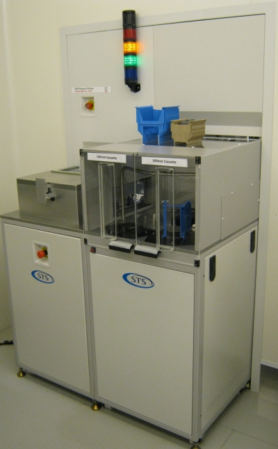
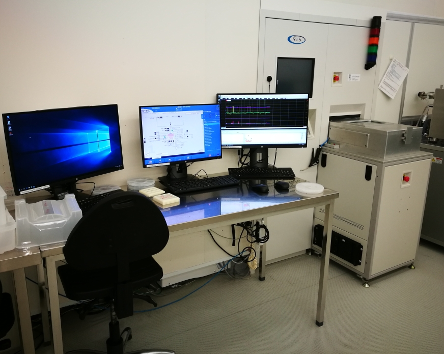
In 2010 Danchip acquired DRIE-Pegasus 1 (at the time called DRIE-Pegasus). As a state-of-the-art etch tool with excellent performance and great flexibility, it grew immensely popular and by 2015 it was apparent that we needed yet another tool to cope with the demand. Therefore, in 2016 Pegasus 2 was acquired from a closed-down lab in Morocco and installed next to Pegasus 1.
Then, in 2017 we got our hands on a twin Pegasus system with cassette to cassette vacuum robot at a very reasonable price from a commerciel fab. The twin Pegasus system (will be called Pegasus 3 and 4) will be installed at the old cluster 2 location in cleanroom C1 from August 2018 onwards.
The Bosch process
The DRIE Pegasus tools are state-of-art silicon dry etchers that offer outstanding performance in terms of etch rate, uniformity etc. They use the so-called Bosch process to achieve excellent control of the etched features. Click HERE for more fundamental information of the system. As of 2017, completing the Dry Etch TPT course is mandatory for all new users. On the TPT web page you will find a version of the latest lecture slides - here you will find information as well.
The user manual(s), quality control procedure(s) and results, user APV(s), technical information and contact information can be found in LabManager:
Equipment info in LabManager
Process information
SPTS process notation
Describing a process recipe on the Pegasus may sometimes be difficult because of the great flexibility of the instrument. A compact and precise notation is therefore required for the recipes. Click here to find a short description of the official SPTS notation.
Hardware changes
A few hardware modifications have been made on the Pegasus since it was installed in 2010. The changes are listed below.
Other etch processes
More processes, such as for DUV resist, are currently being developed, but they are not quite 'ready for publication' at LabAdviser so please contact Jonas (mailto:jml@danchip.dtu.dk) for more information.
Advanced Processing - Henri Jansen style
- Etch high aspect ratio silicon microstructures
- Etch 3 dimensional silicon microstructures
- Etch black silicon
- Using OES to monitor etch process
Wafer bonding
To find information on how to bond wafers or chips to a carrier wafer, click here.
Acceptance test
The instrument was opened for users in April 2010 when the acceptance test was signed. This was based on the performance of five standard recipes (A, B, C, D and SOI) that are further examined below. The acceptance test report is found here.
Characterisation of etched trenches
Comparing differences in etched trenches requires a set of common parameters for each trench. Click here to find more information about the parameters used on the DRIE-Pegasus process development.
Material from SPTS
Internal Danchip Process log
Process log at Danchip [1]
| Equipment | DRIE-Pegasus | |
|---|---|---|
| Purpose | Dry etch of |
|
| Performance | Etch rates |
|
| Uniformity |
| |
| Process parameter range | RF powers |
|
| Gas flows |
| |
| Pressure and temperature |
| |
| Process options |
| |
| Substrates | Batch size |
|
| Allowed materials |
| |
| Possible masking materials |
| |


